UPD78C14L 查看數據表(PDF) - NEC => Renesas Technology
零件编号
产品描述 (功能)
比赛名单
UPD78C14L Datasheet PDF : 52 Pages
| |||
µPD78C14(A)
(Continued)
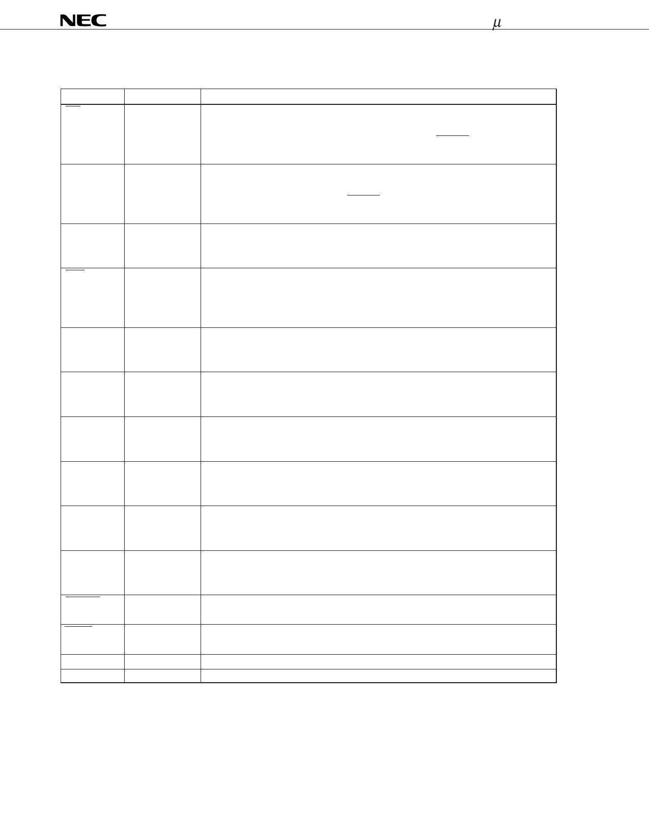
Pin
RD
(Read
Strobe)
ALE
(Address
Latch
Enable)
MODE0
MODE1
(Mode)
NMI
(Non-
Maskable
Interrupt)
INT1
(Interrupt
Request)
AN7-AN0
(Analog
Input)
VAREF
(Reference
Voltage)
AVDD
(Analog
VDD)
AVSS
(Analog
VSS)
X1, X2
(Crystal)
RESET
(Reset)
STOP
(Stop)
VDD
VSS
Input/Output
Output
Output
Input/Output
Input
Function
This is a strobe signal output to read data from external memory. This signal
becomes high level except during the data read machine cycle for external memory.
This signal becomes output high impedance when the RESET signal is low or in
the hardware STOP mode.
This is a strobe signal to externally latch the low-order address information
output to pins PD7-PD0 to access the external memory. This signal becomes
output high impedance when the RESET signal is low or in the hardware STOP
mode.
Set the MODE0 pin to 0 (low level) and MODE1 pin to 1 (high level)Note.
When both pins MODE0 and MODE1 are set to 1Note, these pins synchronize to
the ALE and a control signal is output.
This pin inputs the edge triggering (falling edge) nonmaskable interrupt.
Input
Input
Input
Input
Input
This pin inputs edge triggering (rising edge) maskable interrupt. This pin is also
shared with zero-cross detection pin for AC input.
These eight pins input analog signals for the A/D converter. Pins AN7-AN4 can
be used as edge detection (falling edge) input.
This pin inputs the reference voltage for the A/D converter and controls the
operation for the A/D converter.
Power supply pin for the A/D converter
Ground pin for the A/D converter
These are crystal connecting pins for the system clock oscillation. When a clock
is externally supplied, input it through pin X1. Input the clock to X1 and its reverse
phase to X2.
This pin inputs the active-low reset input signal.
This pin inputs control signal of the hardware STOP mode. When the low level
of this signal is input, the oscillator stops to operate.
Positive power supply pin
Ground pin
Note
Pull-up with the following external resistor:
4 (kΩ) ≤ R ≤ 0.4 tCYC (kΩ)
tCYC (unit: ns)
Example 4 (kΩ) ≤ R ≤ 26 (kΩ): tCYC = 66 (ns) at 15 MHz
4 (kΩ) ≤ R ≤ 33 (kΩ): tCYC = 83 (ns) at 12 MHz
8
Share Link: 