W83195BG-101 查看數據表(PDF) - Winbond
零件编号
产品描述 (功能)
比赛名单
W83195BG-101 Datasheet PDF : 27 Pages
| |||
W83195BR/G-101
STEPLESS FOR INTEL 915/925 CHIPSETS
5.3 Frequency select, and Fixed Frequency Outputs
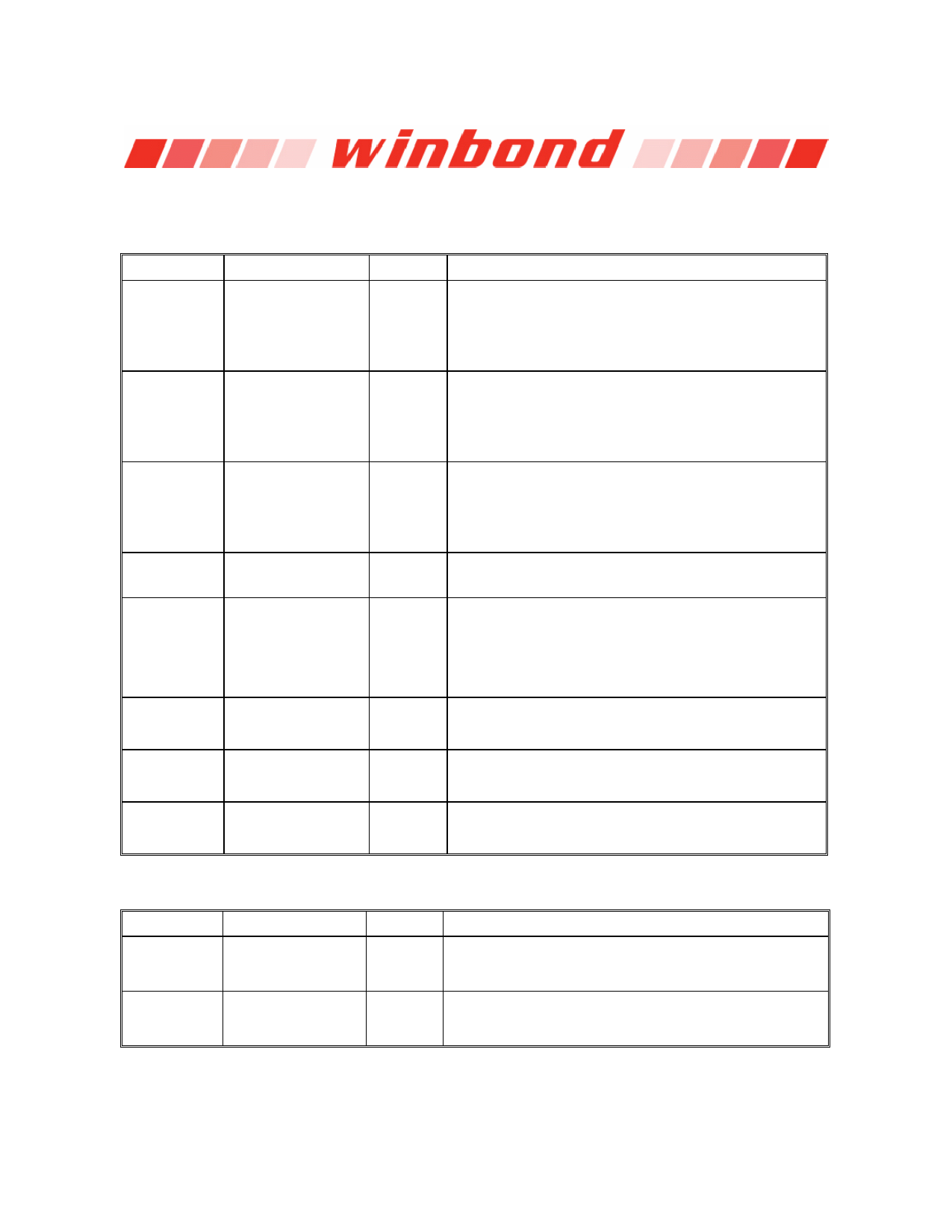
PIN
PIN NAME
TYPE
DESCRIPTION
18
*FS0
INtp120k
Latched input for FS0 at initial power up for H/W
selecting the output frequency. Latched voltage level
refers to Vil_FS and Vih_FS voltage level. This is
internal 120K pull up.
16
*FS1
INtp120k
Latched input for FS1 at initial power up for H/W
selecting the output frequency. Latched voltage level
refers to Vil_FS and Vih_FS voltage level. This is
internal 120K pull up.
53
*FS2
INtp120k
Latched input for FS2 at initial power up for H/W
selecting the output frequency. Latched voltage level
refers to Vil_FS and Vih_FS voltage level. This is
internal 120K pull up.
52
REF0
OUT 3.3V REF0 14.318MHz clock output.
&FS3
INtd120k
Latched input for FS3 at initial power up for H/W
selecting the output frequency. Latched voltage level
refers to Vil_FS and Vih_FS voltage level. This is
internal 120K pull down.
12
48MHz
14,15 DOTT/C_96MHz
26,27 SRCT/C4_SATA
OUT 48MHz clock output for USB.
OUT
0.7V current mode 96MHz differential clock outputs for
DOT
OUT
0.7V current mode 100MHz differential clock outputs
for SATA
5.4 I2C Control Interface
PIN
PIN NAME
47
*SDATA
46
*SCLK
TYPE
I/OD
DESCRIPTION
Serial data of I2C 2-wire control interface with internal
pull-up resistor.
IN
Serial clock of I2C 2-wire control interface with internal
pull-up resistor.
Publication Release Date: March 2006
-5-
Revision 0.7
Share Link: 