W48S87-72X 查看數據表(PDF) - Cypress Semiconductor
零件编号
产品描述 (功能)
比赛名单
W48S87-72X Datasheet PDF : 19 Pages
| |||
W48S87-72
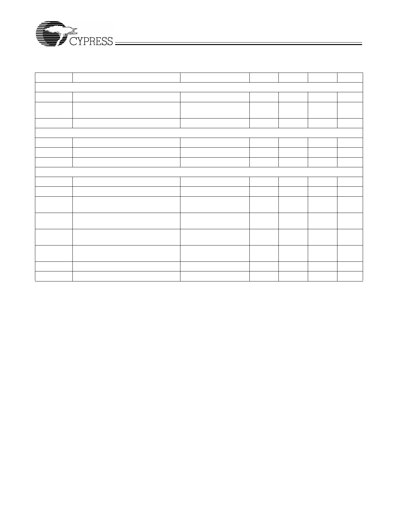
DC Electrical Characteristics: (continued)
TA = 0°C to +70°C, VDDQ3 = 3.3V±5% (3.135–3.465V) fXTL = 14.31818 MHz, VDDQ2 = 2.5±5%
Parameter
Description
Test Condition
Min.
Typ.
Max.
Unit
Crystal Oscillator
VTH
X1 Input Threshold Voltage[6]
CLOAD
Load Capacitance, Imposed on
External Crystal[7]
CIN,X1
X1 Input Capacitance[8]
Pin Capacitance/Inductance
VDD = 3.3V
Pin X2 unconnected
1.65
V
14
pF
28
pF
CIN
Input Pin Capacitance
COUT
Output Pin Capacitance
LIN
Input Pin Inductance
Serial Input Port
Except X1 and X2
5
pF
6
pF
7
nH
VIL
Input Low Voltage
VIH
Input High Voltage
IIL
Input Low Current
VDD = 3.3V
0.4
0.3VDD
V
VDD = 3.3V
0.7VDD
2.4
V
No internal pull-up/down
on SCLOCK
10
10
µA
IIH
Input High Current
No internal pull-up/down
on SCLOCK
10
10
µA
IOL
Sink Current into SDATA or SCLOCK, IOL = 0.3VDD
Open Drain N-Channel Device On
5
10
15
mA
CIN
Input Capacitance of SDATA and
SCLOCK
5
10
pF
CSDATA
Total Capacitance of SDATA Bus
400
pF
CSCLOCK
Total Capacitance of SCLOCK Bus
400
pF
Notes:
6. X1 input threshold voltage (typical) is VDDQ3/2.
7. The W48S87-72 contains an internal crystal load capacitor between pin X1 and ground and another between pin X2 and ground. Total load placed on crystal
is 14 pF; this includes typical stray capacitance of short PCB traces to crystal.
8. X1 input capacitance is applicable when driving X1 with an external clock source (X2 is left unconnected).
13
Share Link: 