CXD2044Q 查看數據表(PDF) - Sony Semiconductor
零件编号
产品描述 (功能)
比赛名单
CXD2044Q Datasheet PDF : 12 Pages
| |||
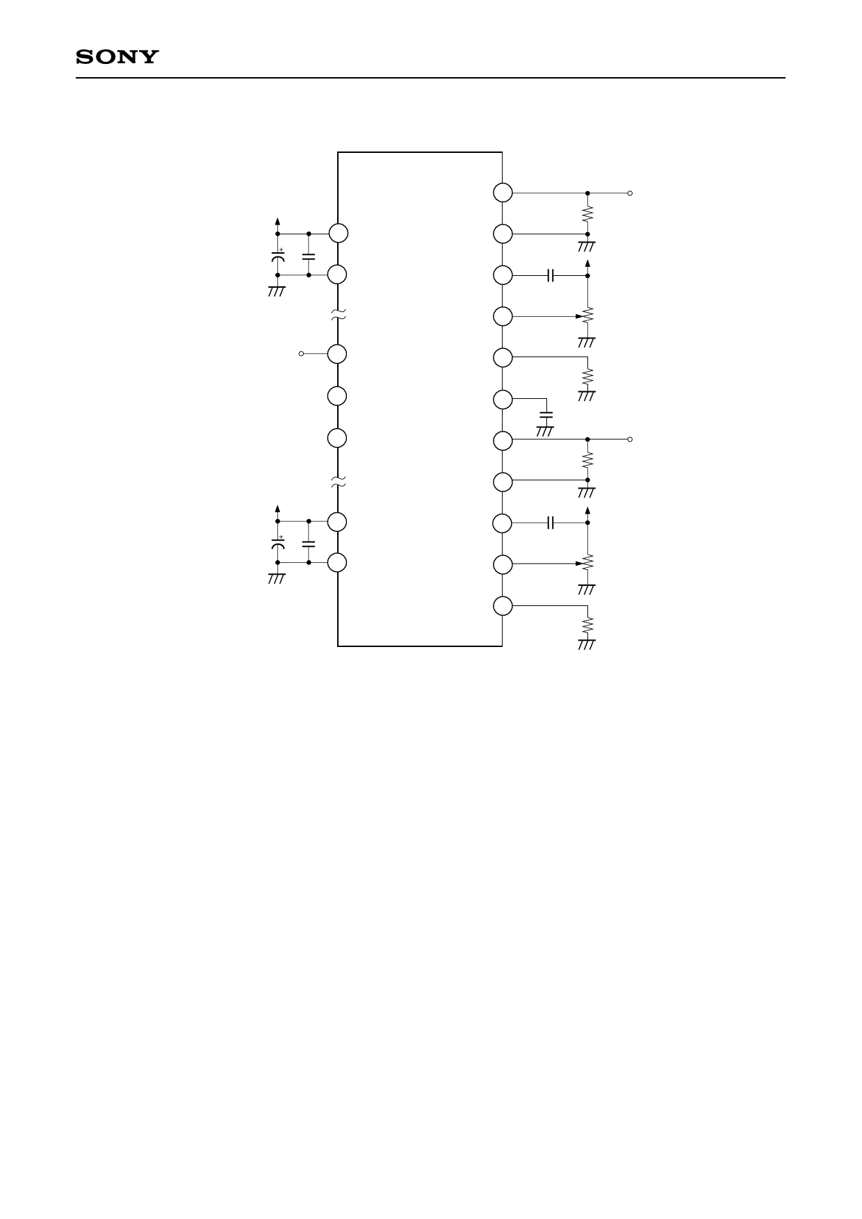
Application Circuit for the D/A Converter Block
CXD2044Q
0.1µ
29 YVDD
35 YVSS
CLOCK
15 MCK
DVDD
DVSS
0.1µ
37 CVDD
43 CVSS
AYO 31
XAYO 30
0.1µ
YVG 32
Y OUTPUT
200 (R)
YVRF 33
1K
YIRF 34
VB 36
ACO 39
XACO 38
CVG 40
3.3k (R')
0.1µ
C OUTPUT
200 (R)
0.1µ
CVRF 41
1K
CIRF 42
3.3k (R')
• Method of selecting the output resistor
The CXD2044Q has a built-in current output type D/A converter. To obtain the output voltages, connect
resistors to the AYO and ACO pins.
The specs are as follows: output full-scale voltage VFS = 0.5 to 2.0 [V], output full-scale current IFS = 0 to
15 [mA].
Calculate the output resistance value using the relationship VFS = IFS × R. In addition, connect a resistor of 16
times the output resistor to the reference current pin (YIRF, CIRF). In case this results in a non-existent
value, use a resistance value as close to the calculated value as possible.
Note that, at this time, VFS = VRF × 16R/R' (VRF: Pin voltage of YVRF and CVRF). Here, R is the resistor
connected to AYO/ACO, and R' is the resistor connected to YIRF/CIRF. Power consumption can be reduced
by using higher resistance values for the R, but the glitch energy and data settling time increase
contrastingly. Set the optimum values according to the system applications.
• VDD, Vss
Separate the analog and digital systems around the device to reduce the effects of noise. YVDD and CVDD
are by-passed to YVss and CVss, respectively, as close to each other as possible through ceramic
capacitors of approximately 0.1µF.
– 10 –
Share Link: 