CXD2044Q 查看數據表(PDF) - Sony Semiconductor
零件编号
产品描述 (功能)
比赛名单
CXD2044Q Datasheet PDF : 12 Pages
| |||
CXD2044Q
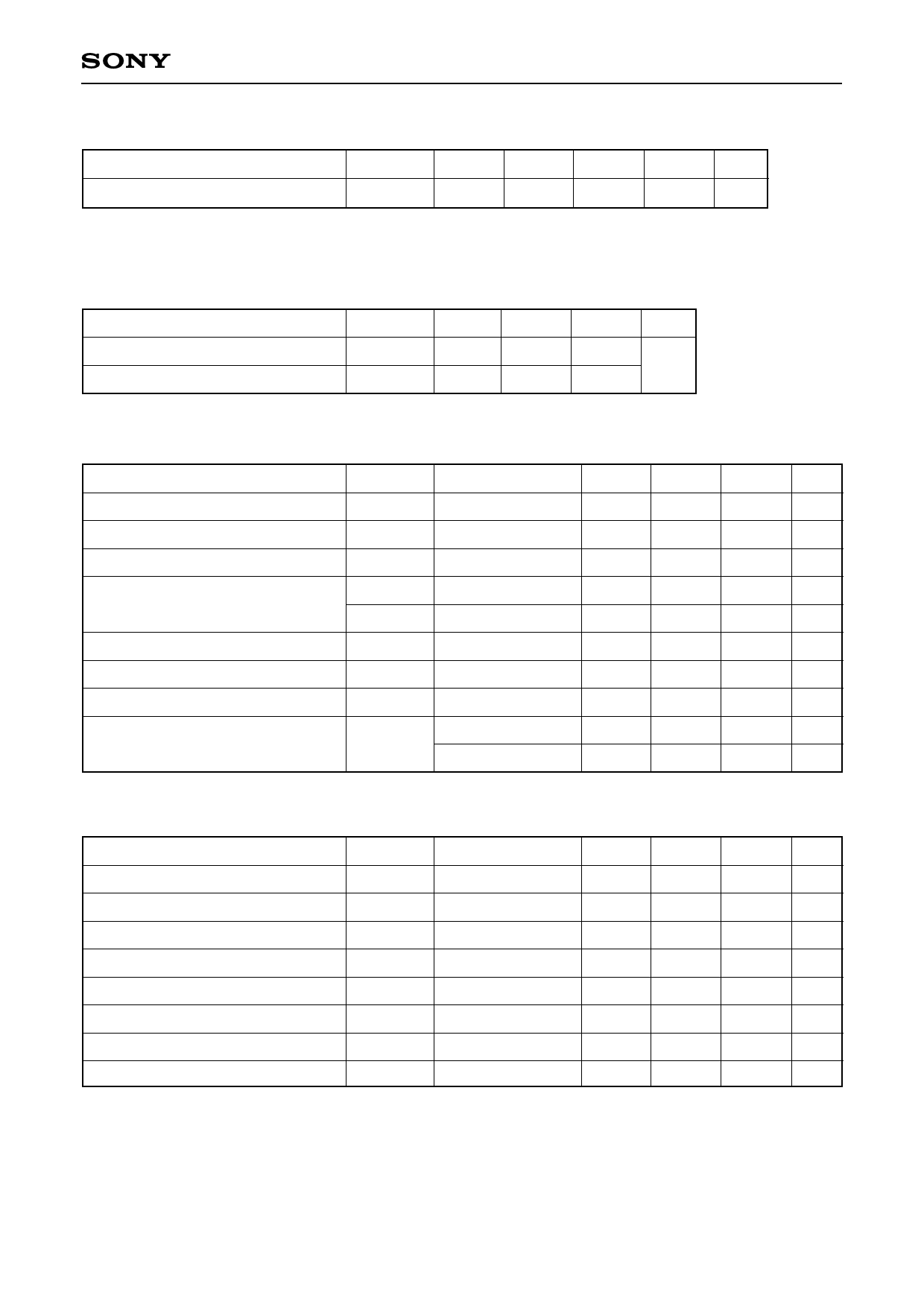
Clock Frequency
(VDD = 4.75 to 5.25V, VSS = 0V, Ta = –20 to +75°C)
Input pin
Pin No. Symbol Min.
OCLK, MCK, ADCK
11, 15, 16
f
—
∗1 fsc = 3.58MHz (NTSC), 4.43MHz (PAL)
Typ.
4fsc∗1
Max.
—
Unit
MHz
I/O Pin Capacitance
Item
Input pin capacitance
Output pin capacitance
(Ta = 25°C, f = 1MHz, VIN = VOUT = 0V)
Symbol
CIN
COUT
Min.
—
—
Typ.
—
—
Max. Unit
9
pF
11
Internal 8-bit ADC Characteristics
Item
Resolution
Max. conversion speed
Analog input bandwidth
Self bias
Output data delay
Differential linearity error
Integral linearity error
Clamp offset voltage
Symbol
Conditions
n
fmax
BW
–3dB
VRB
VRT–VRB
tpd
ED
EL
VREF = VRB
EOC
VREF = VRT
(VDD = 5V, Ta = 25°C, f = 10MHz)
Min.
Typ.
Max. Unit
—
8
—
bit
18
—
— MSPS
—
18
— MHz
0.48 0.52
0.56
V
1.96 2.08
2.22
V
—
—
45
ns
–1.0
—
+1.0 LSB
–3.0
—
+3.0 LSB
–20
0
+20 mV
–30
–10
+10 mV
Internal 8-bit DAC Characteristics
(VDD = 5V, VRF = 2V, RIRF = 3.3kΩ, R = 200Ω, Ta = 25°C, f = 10MHz)
Item
Resolution
Max. conversion speed
Differential linearity error
Integral linearity error
Output full-scale voltage
Output full-scale current
Output offset voltage
Glitch energy
∗2 R = 75Ω, 1Vp-p output
Symbol
n
fmax
ED
EL
VFS
IFS
VOS
GE
Conditions
∗2
Min.
Typ.
Max. Unit
—
8
—
bit
18
—
— MSPS
–0.8
—
+0.8 LSB
–2.0
—
+2.0 LSB
1.805 1.90 1.995 V
—
9.5
15
mA
—
—
1.0 mV
—
30
— pV-s
–8–
Share Link: 