MC14508BCL 查看數據表(PDF) - Motorola => Freescale
零件编号
产品描述 (功能)
比赛名单
MC14508BCL Datasheet PDF : 7 Pages
| |||
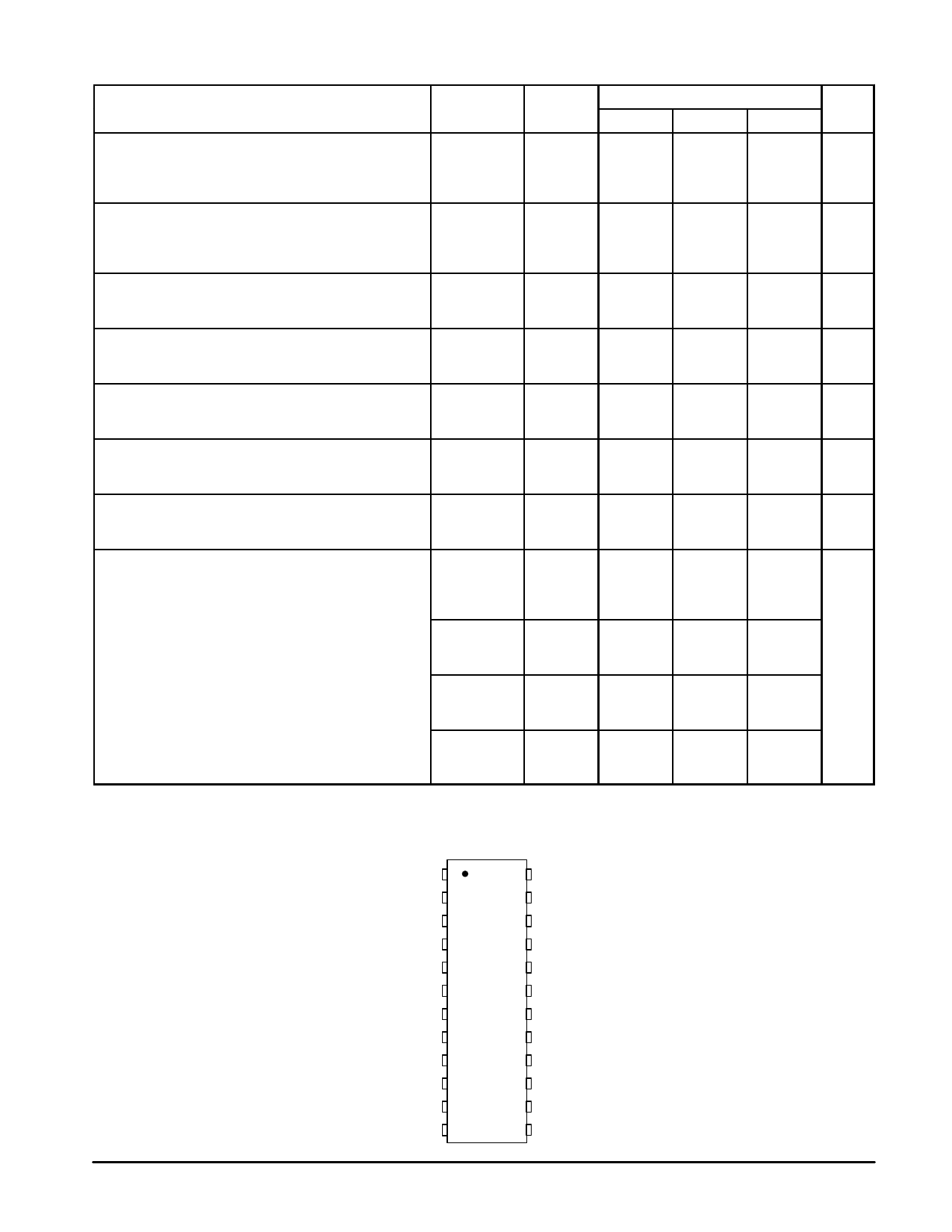
ÎÎÎÎSÎÎÎÎWIÎÎÎÎTCHÎÎÎÎINGÎÎÎÎCHÎÎÎÎARÎÎÎÎACÎÎÎÎTERÎÎÎÎISTÎÎÎÎICSÎÎÎÎ* (CÎÎÎÎL=5ÎÎÎÎ0pFÎÎÎÎ,TAÎÎÎÎ=2ÎÎÎÎ5_CÎÎÎÎ) ÎÎÎÎÎÎÎÎÎÎÎÎÎÎÎÎÎÎÎÎÎÎÎÎÎÎÎÎÎÎÎÎÎÎÎÎAlÎÎÎÎlTypÎÎÎÎes ÎÎÎÎÎÎÎÎÎÎÎÎÎÎÎÎÎÎÎÎÎÎÎÎ
Characteristic
Symbol
VDD
Min
Typ #
Max
Unit
Output Rise and Fall Time
tTLH, tTHL = (1.5 ns/pF) CL + 25 ns
tTLH, tTHL = (0.75 ns/pF) CL + 12.5 ns
tTLH, tTHL = (0.55 ns/pF) CL + 9.5 ns
Propagation Delay Time, Dn or MR to Q
tPLH, tPHL = (1.7 ns/pF) CL + 135 ns
tPLH, tPHL = (0.66 ns/pF) CL + 57 ns
tPLH, tPHL = (0.5 ns/pF) CL + 35 ns
Master Reset Pulse Width
tTLH, tTHL
ns
5.0
—
100
200
10
—
50
100
15
—
40
80
tPLH, tPHL
ns
5.0
—
220
440
10
—
90
180
15
—
60
120
tWH(R)
5.0
200
100
10
100
50
15
70
35
—
ns
—
—
Master Reset Removal Time
trem
5.0
30
– 15
—
ns
10
25
0
—
15
20
0
—
Strobe Pulse Width
tWH(S)
5.0
140
70
10
70
35
15
40
20
—
ns
—
—
Setup Time
Data to Strobe
tsu
5.0
50
25
—
ns
10
20
10
—
15
10
5.0
—
Hold Time
Strobe to Data
th
5.0
50
20
—
ns
10
35
10
—
15
35
10
—
3–State Propagation Delay Time
Output “1” to High Impedance
tPHZ
ns
5.0
—
55
170
10
—
35
100
15
—
30
70
Output “0” to High Impedance
tPLZ
5.0
—
75
170
10
—
40
100
15
—
35
70
High Impedance to “1” Level
tPZH
5.0
—
80
170
10
—
35
100
15
—
30
70
High Impedance to “0” Level
tPZL
5.0
—
105
210
10
—
50
100
15
—
35
70
* The formulas given are for the typical characteristics only at 25_C.
#Data labelled “Typ” is not to be used for design purposes but is intended as an indication of the IC’s potential performance.
PIN ASSIGNMENT
MRA 1
STA 2
DISA 3
D0A 4
Q0A 5
D1A 6
Q1A 7
D2A 8
Q2A 9
D3A 10
Q3A 11
VSS 12
24 VDD
23 Q3B
22 D3B
21 Q2B
20 D2B
19 Q1B
18 D1B
17 Q0B
16 D0B
15 DISB
14 STB
13 MRB
MC14508B
346
MOTOROLA CMOS LOGIC DATA
Share Link: 