L4903 查看數據表(PDF) - STMicroelectronics
零件编号
产品描述 (功能)
比赛名单
L4903 Datasheet PDF : 8 Pages
| |||
L4903
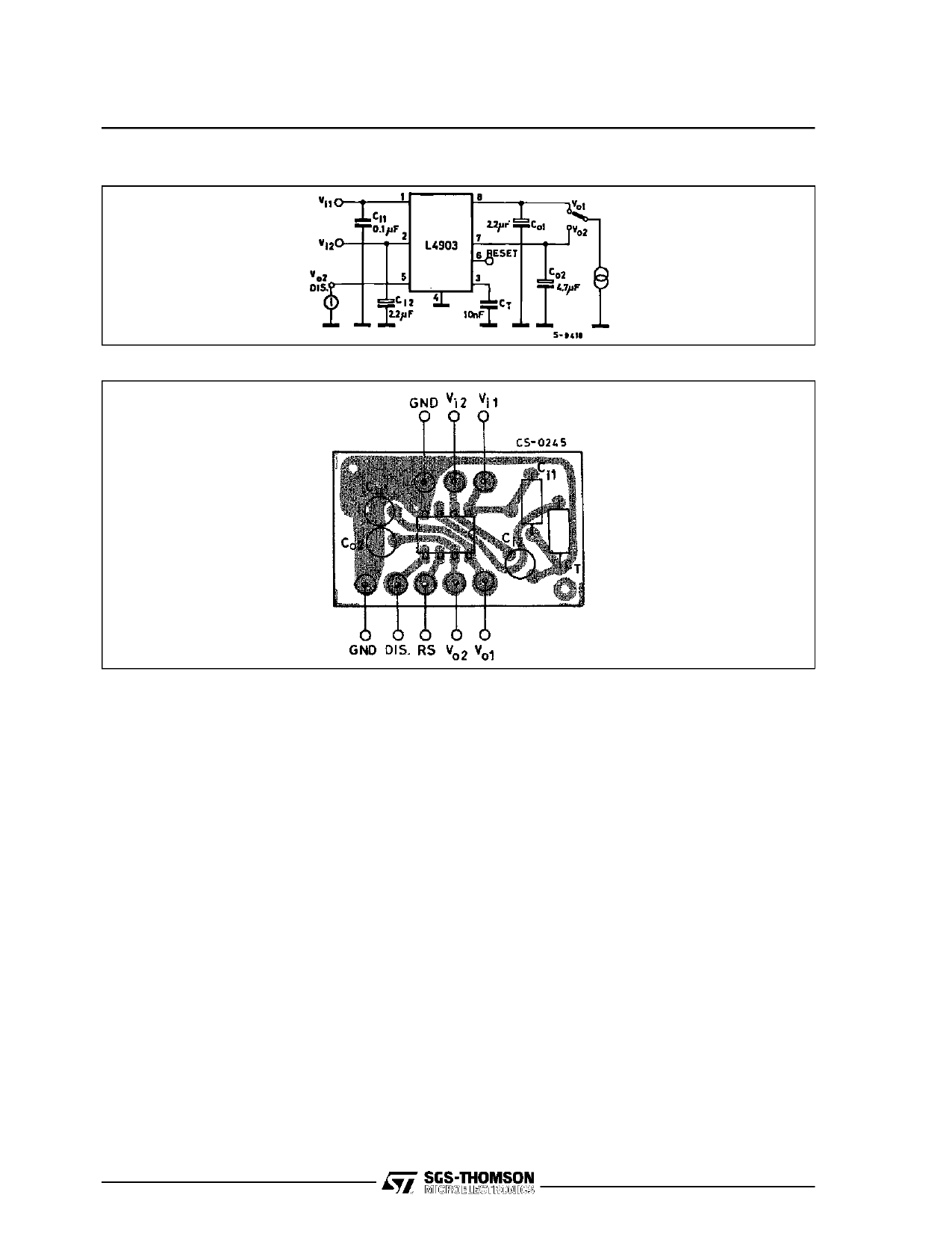
TEST CIRCUIT
Figure 1 : P.C. Board and Components Layout of the Test Circuit
APPLICATION INFORMATION
In power supplies for µP systems it is necessary to
provide power continuously to avoid loss of infor-
mation in memories and in time of day clocks, or to
savedata when the primary supply is removed. The
L4903 makes it very easy to supply such equip-
ments ; it provides two voltage regulators (both 5 V
high precision) with separate inputs plus a reset
output for the data save function and Reg. 2 disable
input.
CIRCUIT OPERATION (see Figure 2)
After switch on Reg. 1 saturates until V01 rises to
the nominal value.
When the input 2 reaches VIT and the output 1 is
higher than VRT the output 2 (V02 and VR) switches
on and the reset output (VR) goes low after a
programmable time TRD (timing capacitor).
V02 is switched at low level and VR at high level
when one of the following conditions occurs ;
- a high level (> VDT) is applied on pin 5 ;
- an input overvoltage ;
- an overload on the output 1 (V01 < VRT) ;
- a switch off (VIN < VIT - VITH) ;
and they start again as before when the condition
4/8
is removed.
An overload on output 2 does not switch Reg. 2,
and does not influence Reg. 1.
The V01 output features :
- 5 V internal reference without voltage divider
between the output and the error comparator
- very low drop series regulator element utilizing
current mirrors
permit high output impedance and then very low
leakage current even in power conditions.
This output may thereforebe used to supply circuits
continuously, such as volatile RAMs, allowing the
use of a back-up battery.
The V02 can supply other non essential 5 V circuits
which may be powered down when the system is
inactive, or that must be powered down to prevent
uncorrect operation for supply voltages below the
minimum value.
The reset output can beused as a ”POWER DOWN
INTERRUPT”, permitting RAM access only in cor-
rect power conditions, or as a ”BACK-UP ENABLE”
to transfer data into in a NV SHADOW MEMORY
when the supply is interrupted.
The disable function can be used for remote on/off
control of circuits connected to the V02 output.
Share Link: 