L4903 查看數據表(PDF) - STMicroelectronics
零件编号
产品描述 (功能)
比赛名单
L4903 Datasheet PDF : 8 Pages
| |||
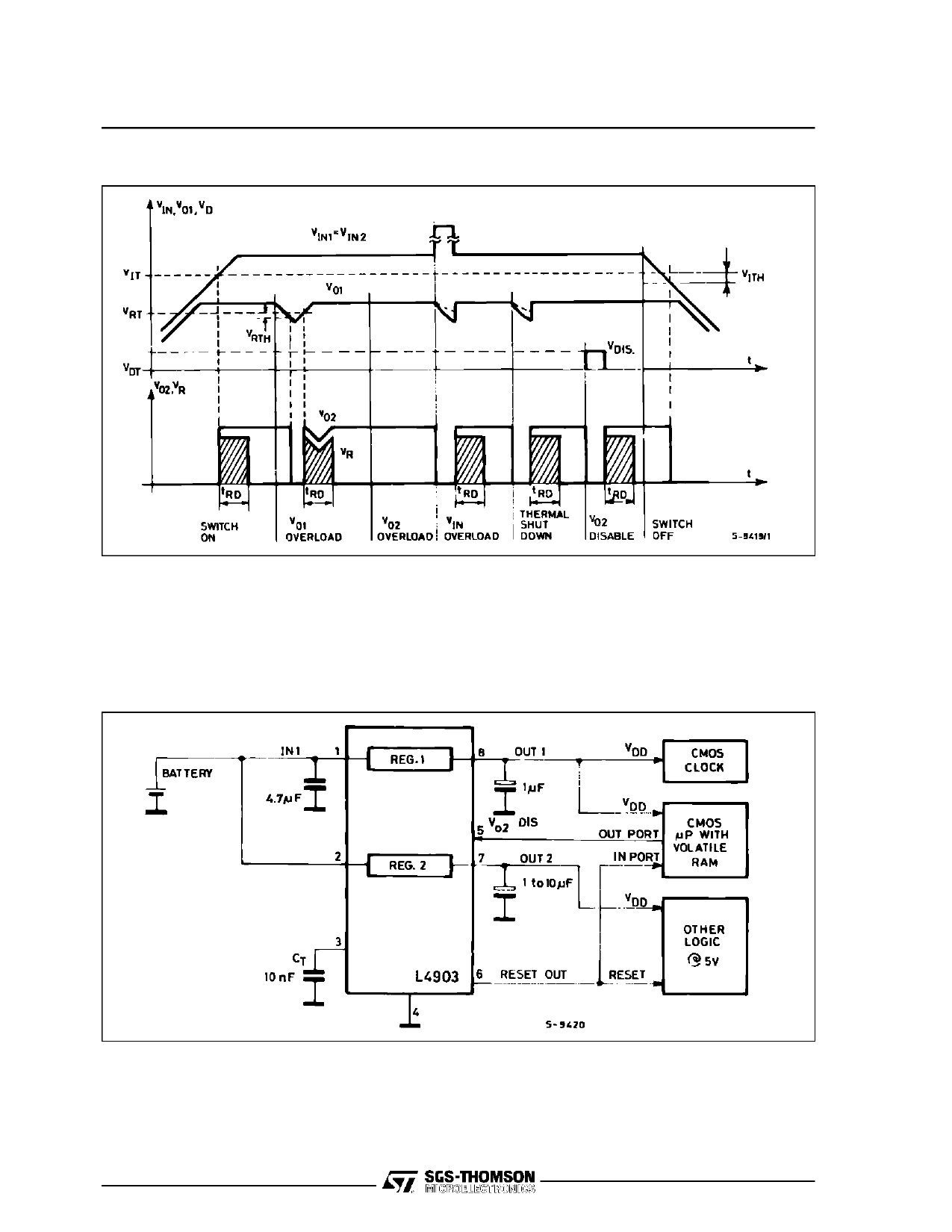
Figure 2
L4903
APPLICATION SUGGESTION
Figure 3 illustrates how the L4903’s disable input
may be used in a CMOS µComputer application.
The V01 regulator (low consumption) supply perma-
nently a CMOS time of day clock and a CMOS
computer chip with volatile memory. V02 output,
Figure 3
supplying non-essential circuits, is turned OFF un-
der control of a µP unit.
Configurations of this type are used in products
where the OFF switch is part of a keyboard
scanned by a micro which operates continuously
even in the OFF state.
5/8
Share Link: 