MAX863EEE 查看數據表(PDF) - Maxim Integrated
零件编号
产品描述 (功能)
比赛名单
MAX863EEE Datasheet PDF : 16 Pages
| |||
Dual, High-Efficiency, PFM, Step-Up
DC-DC Controller
ABSOLUTE MAXIMUM RATINGS
VDD to GND ............................................................-0.3V to +12V
PGND to GND .......................................................-0.3V to +0.3V
SHDN1, SHDN2, SENSE1, LBO to GND ................-0.3V to +12V
EXT1, EXT2 to PGND..................................-0.3V to (VDD + 0.3V)
FB1, FB2, CS1, CS2, SEL,
LBI, BOOT to GND.................................-0.3V to (VDD + 0.3V)
LBO Continuous Output Current.........................................15mA
EXT1, EXT2 Continuous Output Current .............................50mA
Continuous Power Dissipation (TA = +70°C)
QSOP (derate 8.30mW/°C above +70°C) ...................667mW
Operating Temperature Range
MAX863EEE ....................................................-40°C to +85°C
Junction Temperature ......................................................+150°C
Storage Temperature Range .............................-65°C to +160°C
Lead Temperature (soldering, 10sec) .............................+300°C
Stresses beyond those listed under “Absolute Maximum Ratings” may cause permanent damage to the device. These are stress ratings only, and functional
operation of the device at these or any other conditions beyond those indicated in the operational sections of the specifications is not implied. Exposure to
absolute maximum rating conditions for extended periods may affect device reliability.
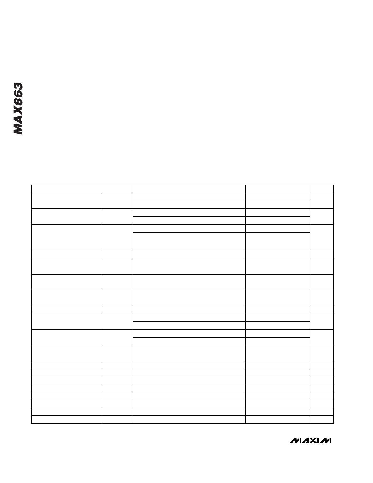
ELECTRICAL CHARACTERISTICS
(VDD = +5V, ILOAD = 0mA, TA = 0°C to +85°C, unless otherwise noted. Typical values are at TA = +25°C.)
PARAMETER
VDD Input Voltage
OUT1 Output Voltage
(Note 3)
Quiescent Current
Shutdown Current
Load Regulation
SYMBOL
VDD
VOUT1
IDD
IDD, SHDN
CONDITIONS
VDD = OUT1 = BOOT (Note 1)
(Note 2)
FB1 = VDD
FB1 = GND
SHDN1 = SHDN2 = VDD, measured from VDD
SHDN1 = VDD, SHDN2 = GND,
measured from VDD
SHDN1 = SHDN2 = GND
VIN = 3.3V, VOUT1 = 5V,
ILOAD = 0mA to 500mA, Figure 2
MIN
1.5
2.7
3.2
4.85
TYP
3.3
5
50
35
40
MAX
11
11
3.4
5.15
85
60
UNITS
V
V
µA
1
µA
mV/A
Line Regulation
FB1, FB2, LBI
Threshold Voltage (Note 4)
FB1, FB2, LBI Input Current
SHDN1, SHDN2, SEL, BOOT
Input High Voltage
SHDN1, SHDN2, SEL, BOOT
Input Low Voltage
SHDN1, SHDN2, SEL, BOOT
Input Current
CS1, CS2 Threshold Voltage
CS1, CS2 Input Current
Maximum Switch On-Time
Minimum Switch Off-Time
EXT Rise/Fall Time (Note 5)
EXT On-Resistance
LBO Leakage Current
LBO Low Level
VFB, VLBI
IFB, ILBI
VIH
VIL
II
VCS
tON
tOFF
ILBO
VLBO,L
VIN = 2.7V to 5V, VOUT1 = 5V,
ILOAD = 300mA, Figure 2
2.7V < VDD < 11V
VDD = 1.5V
2.7V < VDD < 11V
VDD = 1.5V
Logic input = VDD or GND
CLOAD = 1nF, 10% to 90%
VLBO = 11V, VLBI > 1.275V
ILBO,SINK = 1mA, VLBI < 1.225V
8
mV/V
1.225 1.25 1.275
V
2
10
nA
1.6
V
0.7 x VDD
0.4
V
0.2 x VDD
1
µA
85
100
115
mV
1
25
µA
14
17.5
22
µs
1.6
2
2.4
µs
50
ns
5
Ω
1
µA
0.1
0.4
V
2 _______________________________________________________________________________________
Share Link: 