MAX863EEE 查看數據表(PDF) - Maxim Integrated
零件编号
产品描述 (功能)
比赛名单
MAX863EEE Datasheet PDF : 16 Pages
| |||
Dual, High-Efficiency, PFM, Step-Up
DC-DC Controller
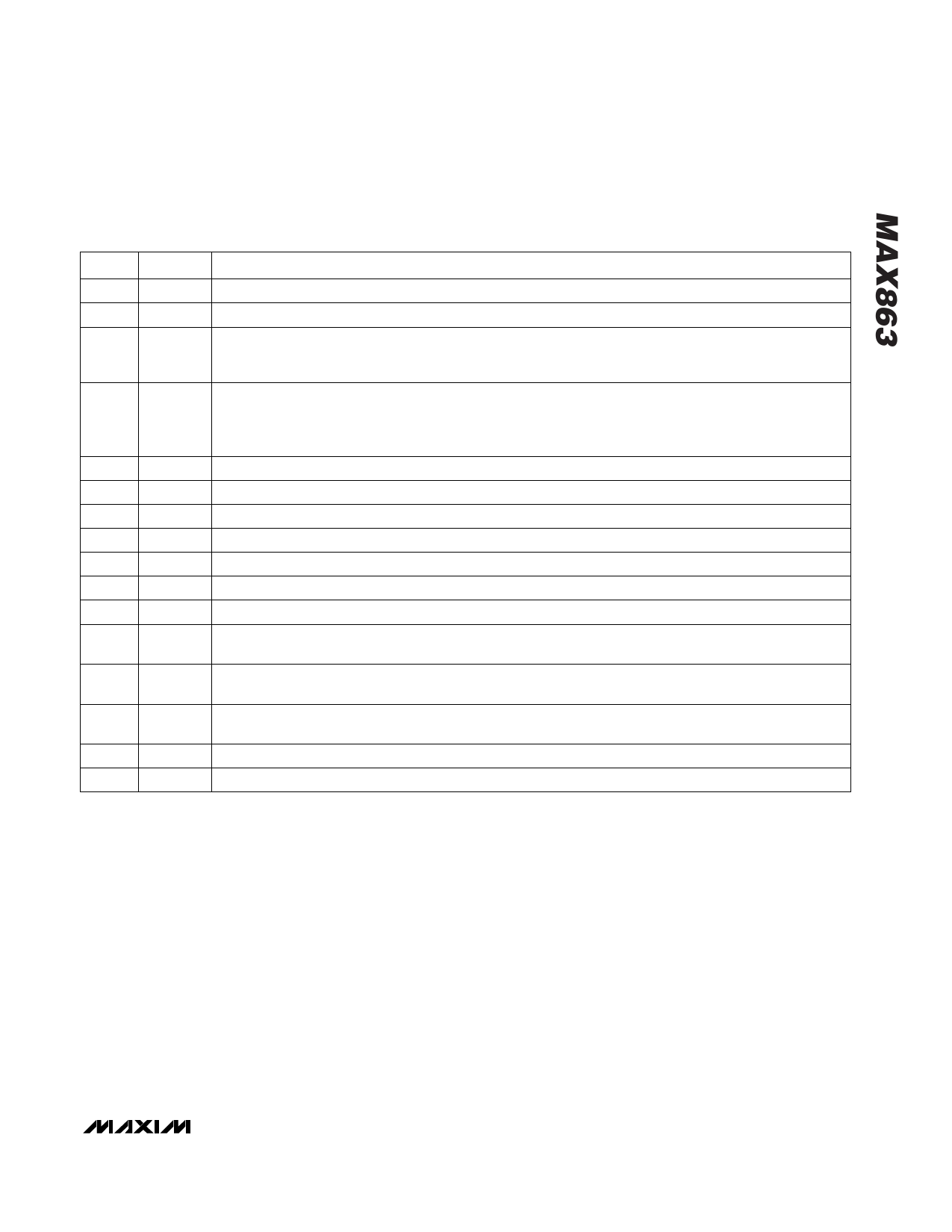
______________________________________________________________Pin Description
PIN
NAME
FUNCTION
1
SENSE1 Feedback Input for DC-DC Controller 1 in Fixed-Output Mode
2
VDD
IC Power-Supply Input
Adjustable Feedback and Preset Output Voltage Selection Input for DC-DC Controller 1. Connect to VDD
3
FB1
for 3.3V preset output or to GND for 5V output. Connect a resistor voltage divider to adjust the output volt-
age. See the section Set the Output Voltage.
Bootstrap Low-Voltage-Oscillator Enable Input. BOOT is an active-high, logic-level input. It enables the
4
BOOT
low-voltage oscillator to allow start-up from input voltages down to 1.5V while in a bootstrapped circuit
configuration. Connect BOOT to GND when in a non-bootstrapped configuration. If BOOT is high, VDD
must be connected to OUT1.
5
CS1
Input to the Current-Sense Comparator of DC-DC Controller 1
6
EXT1
Gate-Drive Output of DC-DC Controller 1. Drives an external N-channel power MOSFET.
7
GND
Analog Ground for Internal Reference, Feedback, and Control Circuits
8
PGND High-Current Ground Return for Internal MOSFET Drivers
9
EXT2
Gate-Drive Output of DC-DC Controller 2. Drives an external N-channel power MOSFET.
10
CS2
Input to the Current-Sense Amplifier of DC-DC Controller 2
11
SHDN1 Active-Low Shutdown Input for DC-DC Controller 1. Connect to VDD for normal operation.
12
FB2
Adjustable Feedback Input for DC-DC Controller 2. Connect a resistor voltage divider to adjust the output
voltage. See the section Set the Output Voltage.
13
LBO
Low-Battery Output. An open-drain N-channel MOSFET output. Sinks current when the voltage on LBI
drops below 1.25V. If unused, connect to GND.
14
LBI
Low-Battery Comparator Input. When the voltage on LBI drops below 1.25V, LBO sinks current. If unused,
connect to GND.
15
SHDN2 Active-Low Shutdown Input for DC-DC Controller 2. Connect to VDD for normal operation.
16
REF
Reference Bypass Input. Connect a 0.1µF ceramic capacitor from REF to GND.
_______________Detailed Description
The MAX863 dual, bi-CMOS, step-up, switch-mode
power-supply controller provides preset 3.3V, 5V, or
adjustable outputs. Its pulse-frequency-modulated
(PFM) control scheme combines the advantages of low
supply current at light loads and high efficiency with
heavy loads. These attributes make the MAX863 ideal
for use in portable battery-powered systems where
small size and low cost are extremely important, and
where low quiescent current and high efficiency are
needed to maximize operational battery life. Use of
external current-sense resistors and MOSFETs allows
the designer to tailor the output current and voltage
capability for a diverse range of applications.
PFM Control Scheme
Each DC-DC controller in the MAX863 uses a one-shot-
sequenced, current-limited PFM design, as shown in
Figure 1. Referring to the Typical Operating Circuit
(Figure 2) and the switching waveforms (Figures 3a–3f),
the circuit works as follows. Output voltage is sensed
by the error comparator using either an internal voltage
divider connected to SENSE1 or an external voltage
divider connected to FB1. When the output voltage
drops, the error comparator sets an internal flip-flop.
The flip-flop turns on an external MOSFET, which allows
inductor current to ramp-up, storing energy in a mag-
netic field.
_______________________________________________________________________________________ 5
Share Link: 