AS1320 查看數據表(PDF) - austriamicrosystems AG
零件编号
产品描述 (功能)
比赛名单
AS1320 Datasheet PDF : 12 Pages
| |||
AS1320
Data Sheet - Detailed Description
8 Detailed Description
The AS1320 is a high-efficiency, compact step-up converter with 35µA quiescent supply current which ensures the
highest efficiency over a wide load range. With a minimum of +1.5V input voltage, the device is well suited for applica-
tions with one- or two-cells, such as lithium ion (Li+), nickel-metal-hydride (NiMH), or alkaline.
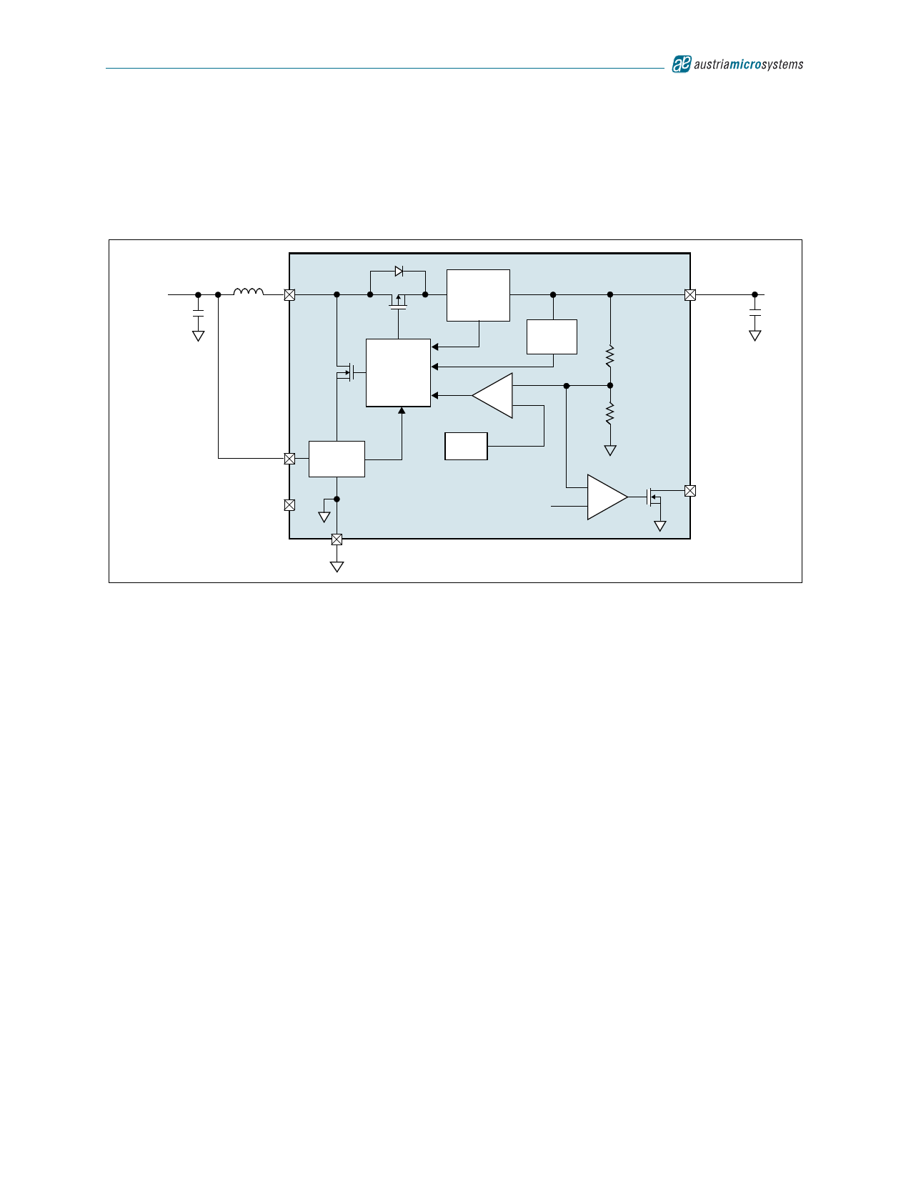
Figure 15. Block Diagram
+1.5 to +3.5V
Battery
CIN
22µF
4
10µH LX
Driver
and
Control
Logic
Zero
Crossing
Detector
Startup
Circuitry
–
+ +1.228V
2
BATT
Current
Limiter
VREF
1
SHDNN
AS1320
–
+1.1V
+
GND 3
5
OUT COUT
22µF
+3.3V
Output
6
RESETN
The input battery is connected to the device through an inductor and an internal P-FET when pin SHDNN is low. In this
state, the step-up converter is off and the voltage drop across the P-FET body diode is eliminated, and the input bat-
tery can be used as a battery-backup or real-time-clock supply.
The built-in synchronous rectifier significantly improves efficiency and reduces PCB circuit size and costs by eliminat-
ing the need for an external Schottky diode.
Control Circuitry
The AS1320 integrated current-limited key circuitry provides low quiescent current and extremely-high efficiency over
a wide VOUT range without the need for an oscillator. Inductor current is limited by the 7µs switch maximum on-time or
by the 0.7A N-channel current limit. At each cycle, the inductor current must ramp down to zero after the on-time
before the next cycle may start. When the error comparator senses that the output has fallen below the regulation
threshold, another cycle begins.
An internal synchronous rectifier eliminates the need for an external Schottky diode, thereby reducing costs and PCB
surface area. As the inductor discharges, the P-channel MOSFET turns on and shunts the MOSFET body diode,
resulting in a significant reduction of the rectifier voltage drop, improving efficiency without external components.
Shutdown
When pin SHDNN is low the AS1320 is switched off and no current is drawn from battery; when pin SHDNN is high the
device is switched on. If SHDNN is driven from a logic-level output, the logic high-level (on) should be referenced to
VOUT to avoid intermittently switching the device on.
Note: If pin SHDNN is not used, it should be connected directly to pin OUT.
In shutdown the battery input is connected to the output through the inductor and the internal synchronous rectifier P-
FET. This allows the input battery to provide backup power for devices such as an idle microcontroller, memory, or real-
time-clock, without the usual diode forward drop. In this way a separate backup battery is not needed.
In cases where there is residual voltage during shutdown, some small amount of energy will be transferred from pin
OUT to pin BATT immediately after shutdown, resulting in a momentary spike of the voltage at pin BATT. The ratio of
CIN and COUT partly determine the size and duration of this spike, as does the current-sink ability of the input device.
www.austriamicrosystems.com
Revision 1.03
7 - 12
Share Link: 