UPD16901GS 查看數據表(PDF) - NEC => Renesas Technology
零件编号
产品描述 (功能)
比赛名单
UPD16901GS Datasheet PDF : 12 Pages
| |||
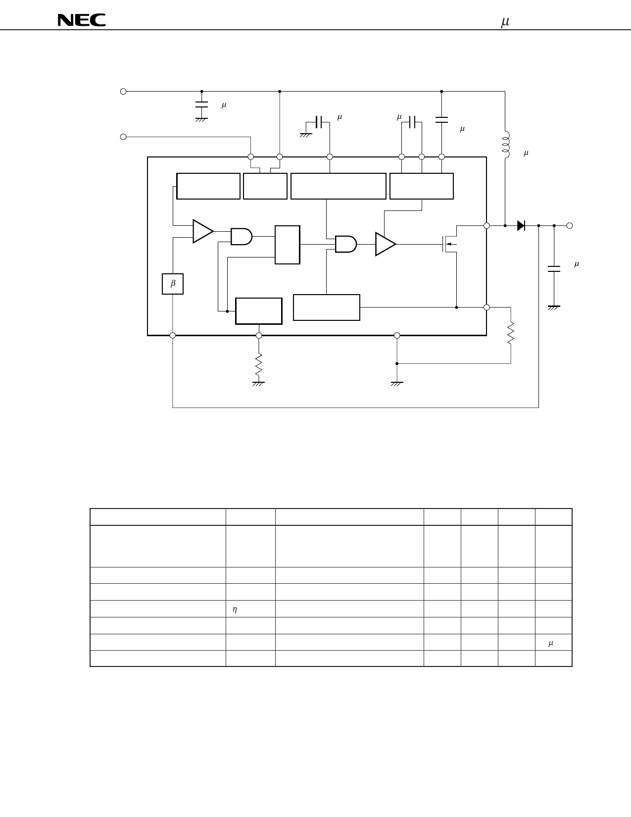
µPD16901
STANDARD CONNECTION DIAGRAM
4.5 V to 5.5 V
ON/OFF
+
CIN
33 µ F
CT 0.1 µ F
VIN
CDLY
0.1 µ F C1
C2
0.1 µ F
C1H C1L C2
L
33 µH
Reference
voltage circuit
Startup Timer latch short-circuit Charge pump
circuit protection circuit
circuit
β
FB
F/F
Oscillation
circuit
Overcurrent
detection circuit
RT
68 kΩ
SW
GND
D
VSW
C.S.
+ 15 µF
COUT
RCS
0.3 Ω
Remark The circuit constants and circuit configuration in this connection diagram are shown for illustrative
purposes and not intended for volume production design.
ELECTRICAL SPECIFICATIONS
(as per standard connection diagram. TA = 25 ˚C, VIN = 5 V, IOUT = 140 mA unless specified otherwise)
Item
Output voltage
Input stability
Load stability
Conversion efficiency
Operating circuit current
Standby circuit current
Startup voltage
Symbol
VOUT
REGIN
REGL
η
ICC
ICC(OFF)
VIN(start-up)
Condition
4.5 V ≤ VIN ≤ 5.5 V
0 mA ≤ IO ≤ 140 mA
0 ˚C ≤TA ≤ 60 ˚C
4.5 V ≤ VIN < 5.5 V
0 mA ≤ IO < 140 mA
IO = 0
ON/OFF pin voltage = 0
MIN. TYP. MAX. Unit
11.52 12.00 12.48
V
0.5
%/V
0.004
%/mA
83
%
3.0
mA
100
µA
3.7
4.3
V
Remark These specifications are reference values confirmed with the standard connection diagram (without
taking account of variations) and are not intended to guarantee the characteristics of the product as a
DC/DC converter.
7
Share Link: 