MCCF33095D 查看數據表(PDF) - Motorola => Freescale
零件编号
产品描述 (功能)
比赛名单
MCCF33095D Datasheet PDF : 12 Pages
| |||
MCCF33095 MC33095
Reflow
The reflow process creates a thermally induced amalgam
of the lead and tin. In the melting process, the surface tension
is equalized causing the melted solder to uniformly ball up as
mentioned earlier.
The ideal reflow oven profile gradually ramps up in
temperature to an initial plateau. The purpose of the plateau
is to establish a near equilibrium temperature just below that
of the solder’s melting temperature. Following the preheat, a
short time and higher temperature excursion is necessary.
This is to ensure adequate melting of the solder materials.
The temperature is then ramped down to room temperature.
An atmosphere of hydrogen is used during the reflow heat
cycle. The hydrogen provides a reducing atmosphere for the
removal of any surface oxides present. The formation or
presence of oxides can cause degradation in the bond
reliability of the product.
During the flip–chip attachment reflow onto the ceramic
substrate host, the created surface tension of the molten
solder aids in the alignment of the chip onto the ceramic
substrate.
Reliability
Motorola is determined to bring high quality and reliable
products to its customers. This is being brought about by
increased automation, in–line Statistical Process Control
(SPC), bump shear strength testing, thermocycling from
– 40° to +140°C, process improvements such as backside
laser marking of the silicon chip, and improved copper
plating techniques.
substrate from external moisture. A commonly used gel for
this purpose is Dow Corning 562. As a final module assembly
step, a cover is recommended to be placed over the ceramic
assembly for further protection of the circuit.
It should be pointed out that the commonly used ceramic
substrate material, though more expensive than other
substrate materials, offers significantly superior thermal
properties. By comparison, the use of ceramic material offers
33 times the thermal advantage of the second best material,
Ceracom. The common FR–4 epoxy material is 100 times
less thermally conductive than ceramic. For applications
where dielectric constants are important and/or heat
dissipation is not of real importance, other less costly
materials can be used. The basic concept of the process is
identical for all flip–chip substrates used.
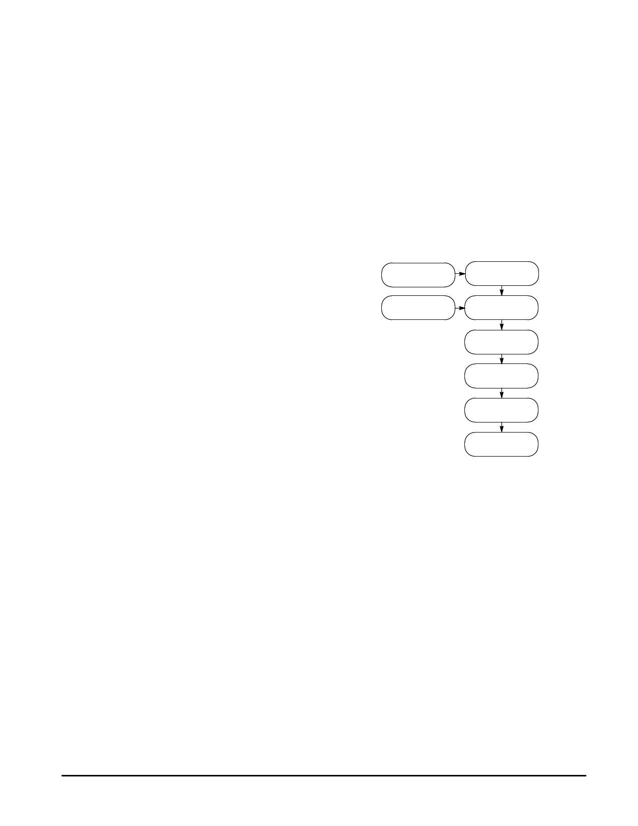
Figure 10. Process Flow Diagram
Printed Circuit
Board (PCB)
Bumping PCB
Bumped Chip
Bumped PCB
on Pallet
Chip Placement
IR Reflow
ATTACHING FLIP–CHIPS ONTO
CERAMIC SUBSTRATES
Overview
The assembly or process of attaching the flip–chip onto a
ceramic substrate is performed by the module fabricator.
Prior to actual assembly, the ceramic substrate should
undergo several process steps. Care should be exercised to
properly orient the flip–chip onto the substrate host in order to
accommodate the appropriate solder bumps. Ideally, the
flip–chip should be removed from the waffle pack with a pick
and place machine utilizing a vacuum pick–up to move the
die onto the ceramic substrate. Any other components to be
reflow soldered onto the substrate can be placed onto the
substrate in a similar manner. Flip–chip assembly onto a
ceramic substrate allows for some passive components,
such as resistors, to be formed directly into the ceramic
substrate circuit pattern itself. With all surface components to
be mounted in place on the ceramic substrate, the assembly
is moved into the furnace where it undergoes a specified
temperature variation to solder all the components onto the
ceramic substrate. This is accomplished by melting
(reflowing) the substrate solder bumps. The resulting
assembly should, after being cooled, be cleaned to remove
any flux residues. If the substrate assembly is to be mounted
into a module, it is recommended that the cavity of the
module be filled with an appropriate silicon gel. The use of a
gel coating helps to seal the individual components on the
Cleaning
Encapsulation
Ceramic Substrate Preparation
The recommended ceramic substrate is aluminum oxide.
These substrates come connected in what is referred to as a
card. This is identical to the concept of die or chips on a wafer.
Each card usually contains 8 to 16 substrates.
Initially, the ceramic should be precleaned with isopropyl
alcohol, followed by freon. The bump pattern is then
transferred onto the substrate using a metal stencil technique
using a palladium silver conducting paste, such as DuPont
9476, through a #325 mesh. Once the pattern is applied, the
substrate is dried for ten minutes at 150°C and then fired for
60 minutes at a temperature increasing to a peak of 850°C for
ten additional minutes. Solder paste is then stenciled onto
the pads.
A metal etched stencil defining the contact areas is
recommended. The use of an etched stencil affords better
solder paste control than does a silk screen. The metal stencil
affords a deposition of a known amount of solder paste,
thereby preventing bridging caused by excess solder usage.
8
MOTOROLA ANALOG IC DEVICE DATA
Share Link: 