TDA9859 查看數據表(PDF) - NXP Semiconductors.
零件编号
产品描述 (功能)
比赛名单
TDA9859 Datasheet PDF : 20 Pages
| |||
Philips Semiconductors
Universal hi-fi audio processor for TV
Preliminary specification
TDA9859
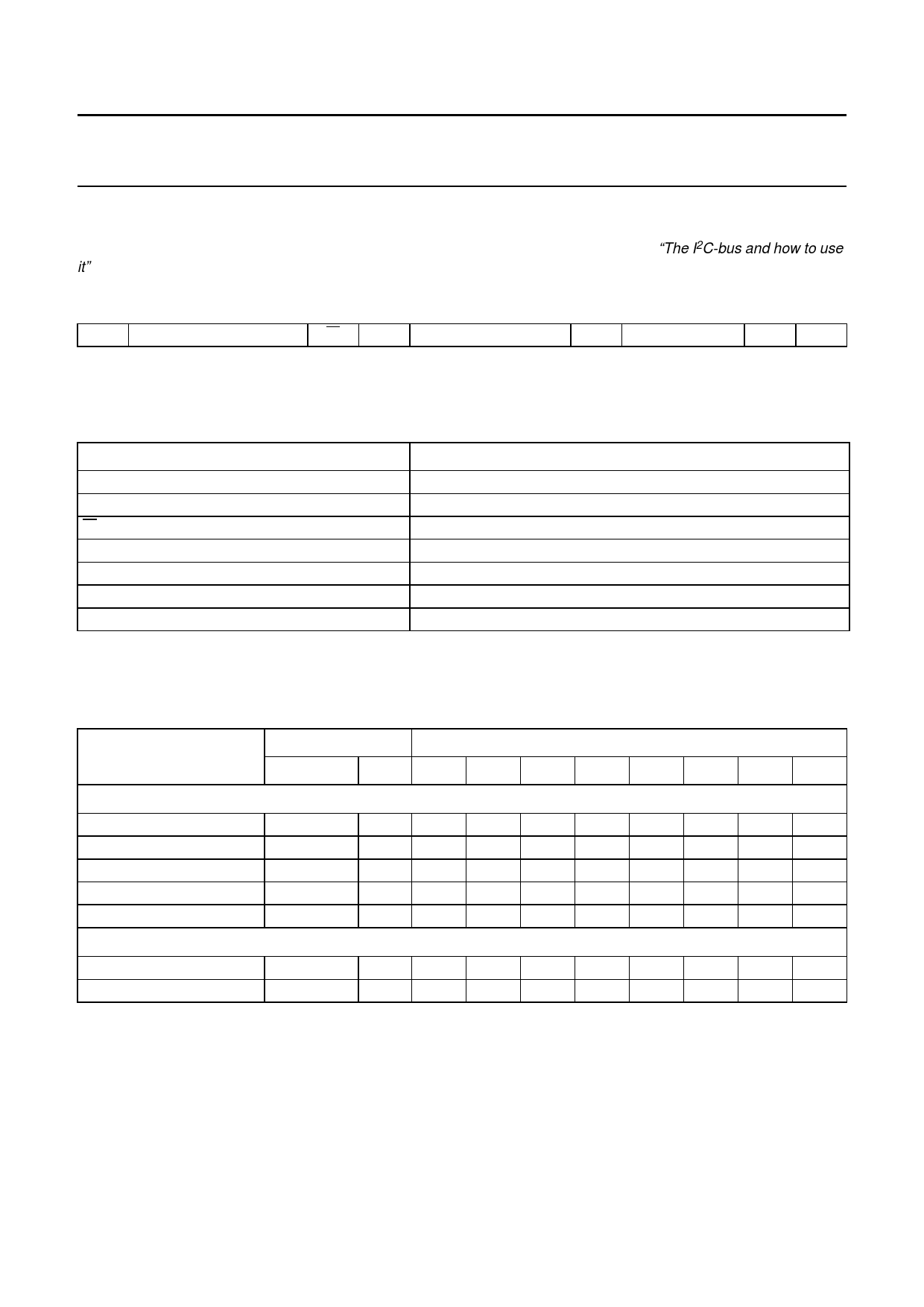
I2C-BUS PROTOCOL
This circuit operates as a slave receiver only. For more information about the I2C-bus, see “The I2C-bus and how to use
it”, order number 9398 393 40011.
I2C-bus format
S
SLAVE ADDRESS
W
A
SUBADDRESS
A
Note
1. Multiple DATA-A (acknowledge) sequences may occur.
DATA(1)
A(1)
P
Table 1 Explanation of I2C-bus format
S
SLAVE ADDRESS
W
A
SUBADDRESS
DATA(1)
P
NAME
DESCRIPTION
START condition (SCL HIGH, SDA HIGH-to-LOW)
100 0000 (V25 = LOW) or 100 0001 (V25 = HIGH)
0
acknowledge (SDA = LOW); generated by the device
subaddress (byte); see Table 2
data byte; see Table 2
STOP condition (SCL = HIGH, SDA = LOW-to-HIGH)
Note
1. If more than 1 byte of DATA is transmitted, then auto-increment of the subaddress is performed by the device.
Table 2 I2C-bus transmission
FUNCTION
SUBADDRESS
DATA BITS
BINARY HEX D7 D6 D5 D4 D3 D2 D1 D0
Loudspeaker channel
Volume control common
Volume control left
Volume control right
Bass control
Treble control
Switching control byte
SCART output(1)
Loudspeaker output
0000 0000 00
0000 0001 01
0000 0010 02
0000 0011 03
0000 0100 04
0000 1000 08
0000 1001 09
0
0 V05 V04 V03 V02 V01 V00
0
0
0 VL4 VL3 VL2 VL1 VL0
0
0
0 VR4 VR3 VR2 VR1 VR0
0
0
0 BA4 BA3 BA2 BA1 BA0
0
0
0
0 TR3 TR2 TR1 TR0
0 MU1 P1 P2 I13 I12 I11 I10
EF2 MU2 EF1 ST I23 I22 I21 I20
Note
1. If auto-increment of the subaddress is used, it is necessary to insert three dummy data words between the treble
control byte and the switching control bytes.
1997 Sep 01
10
Share Link: 