TDA9859 查看數據表(PDF) - NXP Semiconductors.
零件编号
产品描述 (功能)
比赛名单
TDA9859 Datasheet PDF : 20 Pages
| |||
Philips Semiconductors
Universal hi-fi audio processor for TV
Preliminary specification
TDA9859
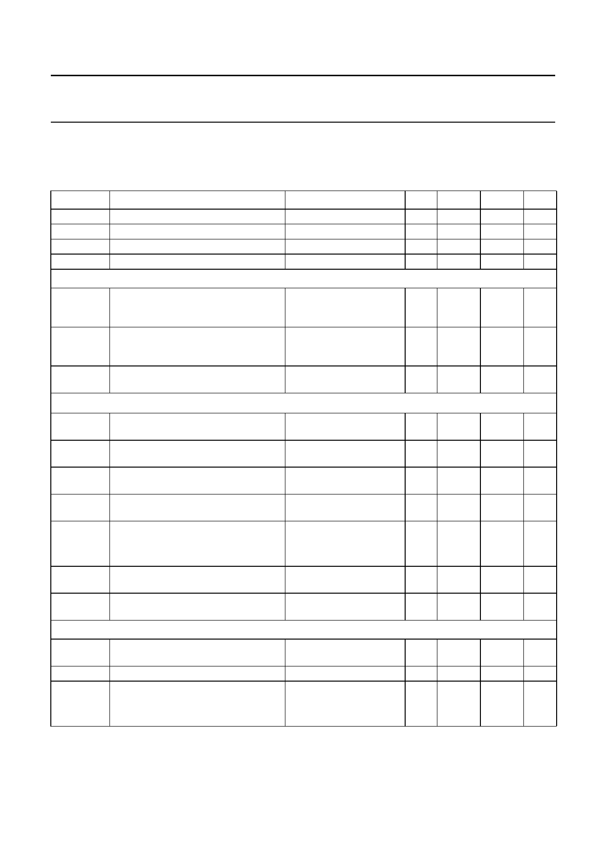
CHARACTERISTICS
VP = 8 V; Tamb = 25 °C; treble and bass in linear positions (0 dB); volume control left/right 0 dB; spatial function,
pseudo-stereo function and forced-mono function in off position and measurements taken in Fig.1; unless otherwise
specified.
SYMBOL
PARAMETER
CONDITIONS
MIN. TYP. MAX. UNIT
VP
supply voltage (pin 6)
IP
supply current (pin 6)
Vref
internal reference voltage
V4
voltage at pin 4
DC voltage on pins
VI
DC input voltage at pins 1, 3, 5, 10, 23,
28, 30 and 32 (inputs SCIN, MIN, LIN
and AIN)
VO
DC output voltage at pins 7, 9, 15, 18,
24, 26 (outputs SCOUT, MOUT
and LOUT)
VC
DC voltage on capacitors (pins 11, 12,
14, 19, 21, 22, 27 and 29)
7.2 8.0
8.8
V
−
25
−
mA
−
0.5VP −
V
−
VP − 0.1 −
V
−
0.5VP −
V
−
0.5VP −
V
−
0.5VP −
V
Audio select switch; line and SCART outputs (controlled via I2C-bus); see Table 4
Vi(rms)
maximum AF input signal on
THD ≤ 0.5% on output
2
−
pins SCIN, MIN and AIN (RMS value) pins
Ri
input resistance (pins SCIN, MIN and
AIN)
20 30
B−0.5 dB
−0.5 dB bandwidth for pins SCOUT,
MOUT and LOUT.
20 −
Vo(rms)
maximum AF output signal on
THD ≤ 0.5%
pins SCOUT and MOUT (RMS value)
2
−
RL
allowed external load resistance
on output (pins MOUT)
on output (pins SCOUT)
Gv
voltage gain from any input to SCART
and MAIN outputs
10 −
5
−
−
0
αcr
switch crosstalk on outputs between unused inputs connected −
90
AF inputs at f = 10 kHz
to ground
−
V
40
kΩ
20 000 Hz
−
V
−
kΩ
−
kΩ
−
dB
−
dB
Volume control common (f = 1 kHz, 55 steps)
Vi(rms)
maximum input signal (RMS value;
pins LIN)
Ri
input resistance (pins LIN)
Gv
volume control common voltage gain
nominal
minimum
Gv = 0; THD ≤ 0.5% on
output pins 15 and 18
2
−
7.5 10
−40 −
−38 −
−
V
−
kΩ
+15
dB
+14
dB
1997 Sep 01
6
Share Link: 