GS88237BB-250V 查看數據表(PDF) - Giga Semiconductor
零件编号
产品描述 (功能)
比赛名单
GS88237BB-250V Datasheet PDF : 28 Pages
| |||
GS88237BB/D-xxxV
VDDQ2 & VDDQ1 Range Logic Levels
VDD Input Low Voltage
VIL
–0.3
—
0.3*VDD
V
1
Notes:
1. The part numbers of Industrial Temperature Range versions end the character “I”. Unless otherwise noted, all performance specifica-
tions quoted are evaluated for worst case in the temperature range marked on the device.
2. Input Under/overshoot voltage must be –2 V > Vi < VDDn+2 V not to exceed 4.6 V maximum, with a pulse width not to exceed 20% tKC.
Recommended Operating Temperatures
Parameter
Symbol Min.
Typ.
Max.
Unit Notes
Ambient Temperature (Commercial Range Versions)
TA
0
25
70
°C
2
Ambient Temperature (Industrial Range Versions)
TA
–40
25
85
°C
2
Notes:
1. The part numbers of Industrial Temperature Range versions end the character “I”. Unless otherwise noted, all performance specifica-
tions quoted are evaluated for worst case in the temperature range marked on the device.
2. Input Under/overshoot voltage must be –2 V > Vi < VDDn+2 V not to exceed 4.6 V maximum, with a pulse width not to exceed 20% tKC.
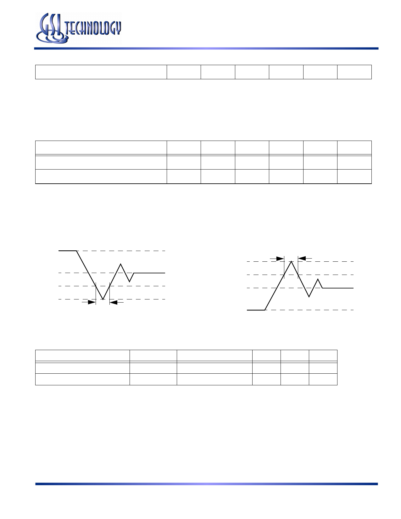
Undershoot Measurement and Timing
VIH
VSS
50%
VSS – 2.0 V
20% tKC
Capacitance
(TA = 25oC, f = 1 MHZ, VDD = 2.5 V)
Parameter
Symbol
Input Capacitance
CIN
Input/Output Capacitance
CI/O
Note:
These parameters are sample tested.
Overshoot Measurement and Timing
VDD + 2.0 V
50%
20% tKC
VDD
VIL
Test conditions
VIN = 0 V
VOUT = 0 V
Typ. Max. Unit
4
5
pF
6
7
pF
Rev: 1.04 6/2006
12/28
Specifications cited are subject to change without notice. For latest documentation see http://www.gsitechnology.com.
© 2003, GSI Technology
Share Link: 