TDA9851T/V1 查看數據表(PDF) - Philips Electronics
零件编号
产品描述 (功能)
比赛名单
TDA9851T/V1 Datasheet PDF : 20 Pages
| |||
Philips Semiconductors
I2C-bus controlled economic BTSC stereo
decoder
Product specification
TDA9851
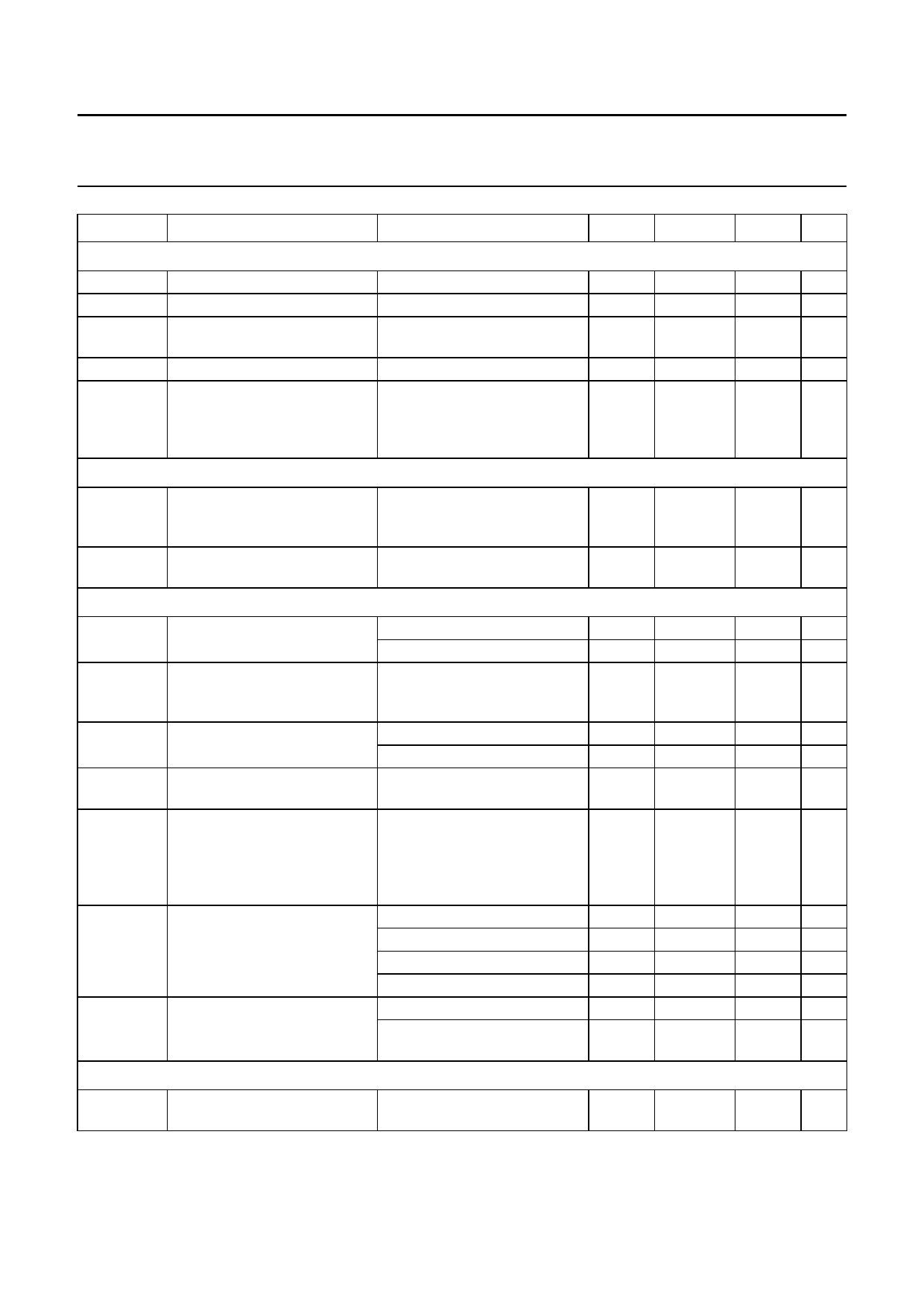
SYMBOL
PARAMETER
CONDITIONS
MIN.
TYP.
MAX. UNIT
Outputs OUTL and OUTR
Zo
output impedance
VO
DC output voltage
RL
output load resistance
(AC-coupled)
CL
output load capacitance
αct
crosstalk SAP into L and R
100% modulation;
fmod = 1 kHz; SAP;
mode selector switched to
stereo
−
80
0.45VCC 0.5VCC
5
−
−
−
50
70
120
Ω
0.55VCC V
−
kΩ
2.5
nF
−
dB
VCA
Is
Relrate
nominal timing current for
Is can be measured at pin TW 6.5
8
nominal release rate of VCA via current meter connected to
detector
0.5VCC + 1 V
nominal detector release rate nominal timing current and
−
125
external capacitor values
9.5
µA
−
dB/s
Automatic volume level control
Gv
Gstep
voltage gain
maximum boost; note 2
5
6
maximum attenuation; note 2 14
15
equivalent step width between
the input stages (soft switching
system)
−
1.5
7
dB
16
dB
−
dB
Viop(rms)
input voltage (RMS value)
maximum boost; note 2
−
0.1
−
V
maximum attenuation; note 2 −
1.125
−
V
Vo(rms)
output voltage in AVL
operation (RMS value)
160
200
250
mV
Voffset(DC)
DC offset voltage between
different gain steps
voltage at pin CAV
7.0 to 6.83 V or
6.83 to 6.61 V or
6.61 to 5.83 V or
5.83 to 3.1 V; note 3
−
−
20
mV
Ratt
discharge resistors for attack AT1 = 0; AT2 = 0; note 4
340
420
520
Ω
time constant
AT1 = 1; AT2 = 0; note 4
590
730
910
Ω
AT1 = 0; AT2 = 1; note 4
0.96 1.2
1.5
kΩ
AT1 = 1; AT2 = 1; note 4
1.7
2.1
2.6
kΩ
Idec
charge current for decay time normal mode; CCD = 0; note 5 1.6
2.0
2.4
µA
power-on speed-up; CCD = 1; −
30
note 5
−
µA
Muting at power supply voltage drop for OUTR and OUTL
∆VCC
supply voltage drop for mute
active
−
VCAP − 0.7 −
V
1997 Nov 12
8
Share Link: 