LIS2L02AS 查看數據表(PDF) - STMicroelectronics
零件编号
产品描述 (功能)
比赛名单
LIS2L02AS Datasheet PDF : 6 Pages
| |||
LIS2L02AS
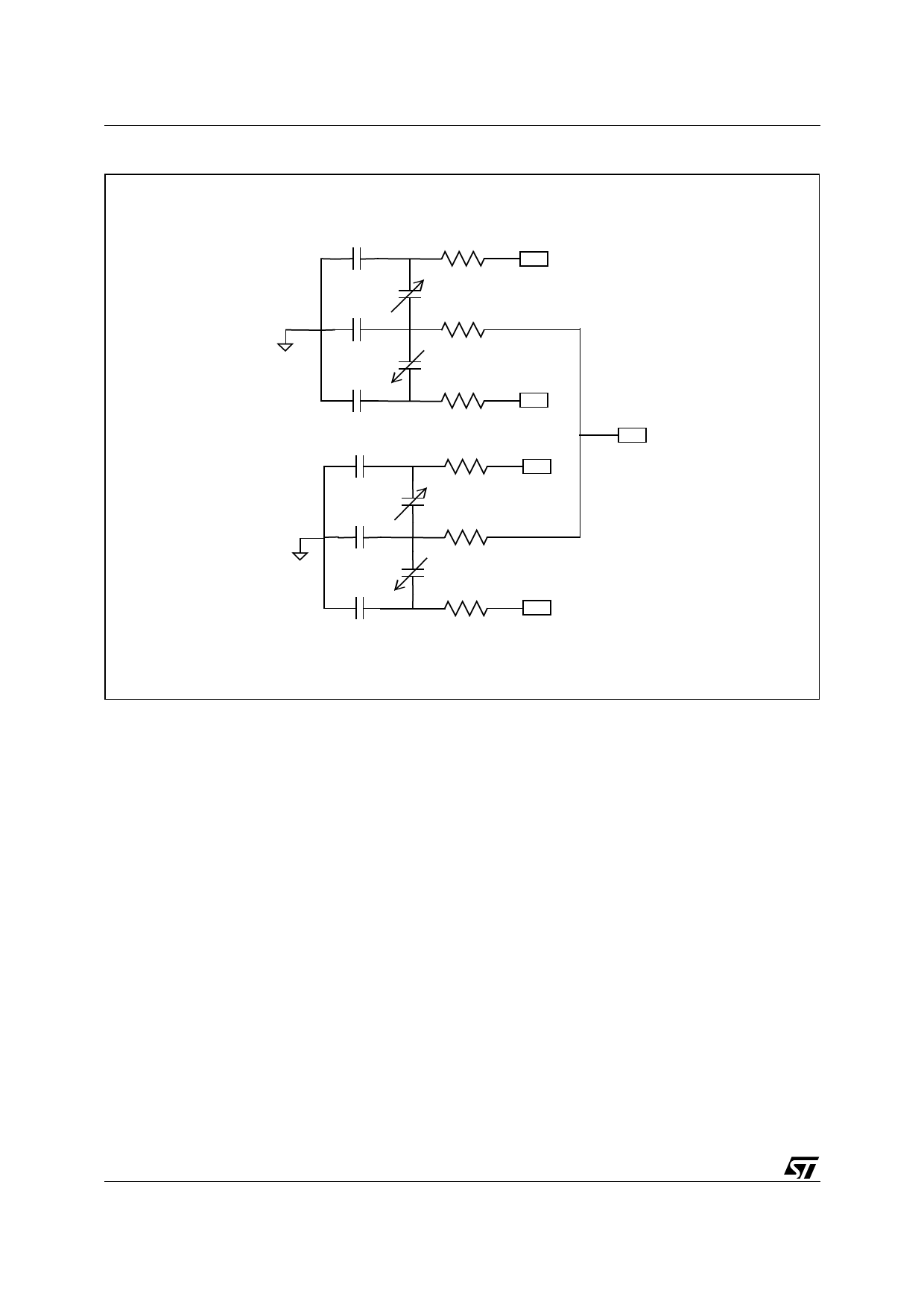
Figure 1. Equivalent electrical circuit
Cps1
Rs1
S1x
Cs1x
Cpr
Rr
Cs2x
Cps2
Cps1
S2x
Rs2
rot
Rs1
S1y
Cs1y
Cpr
Rr
Cs2y
Cps2
S2y
Rs2
1.2 IC Interface
The complete signal processing uses a fully differential structure, while the final stage converts the differential
signal into a single-ended one to be compatible with the external world.
The first stage is a low-noise capacitive amplifier that implements a Correlated Double Sampling (CDS) at its
output to cancel the offset and the 1/f noise. The produced signal is then sent to two different S&Hs, one for
each channel, and made available to the outside.
The low noise input amplifier operates at 200 kHz while the two S&Hs operate at a sampling frequency of 66
kHz. This allows a large oversampling ratio, which leads to in-band noise reduction and to an accurate output
waveform.
All the analog parameters (output offset voltage and sensitivity) are ratiometric to the voltage supply. Increasing
or decreasing the voltage supply, the sensitivity and the offset will increase or decrease linearly. The feature
provides the cancellation of the error related to the voltage supply along an analog to digital conversion chain.
1.3 Factory calibration
The IC interface is factory calibrated to provide to the final user a device ready to operate. The parameters which
are trimmed are: gain, offset, common mode and internal clock frequency.
The trimming values are stored inside the device by a poly-fuse structure. Any time the device is turned on, the
memorized bits are downloaded into the registers to be employed during the normal operation. The poly-fuse
approach allows the final user to utilize the device without any need for further calibration
4/6
Share Link: 