ADG528A 查看數據表(PDF) - Analog Devices
零件编号
产品描述 (功能)
比赛名单
ADG528A Datasheet PDF : 12 Pages
| |||
ADG528A/ADG529A
TRUTH TABLES
A2 A1 A0 EN WR RS ON SWITCH PAIR
XXXX
XXXX X
XXX0 0
0001 0
0011 0
0101 0
0111 0
1001 0
1011 0
1101 0
1111 0
1 Retains Previous Switch Condition
0 NONE (Address and Enable
Latches Cleared)
1 NONE
11
12
13
14
15
16
17
18
X = Don’t Care
ADG528A
A1 A0 EN WR RS ON SWITCH PAIR
XXX
1 Retains Previous Switch Condition
X X X X 0 NONE (Address and Enable Latches
Cleared)
X X 0 0 1 NONE
001 0 1 1
011 0 1 2
101 0 1 3
111 0 1 4
X = Don’t Care
ADG529A
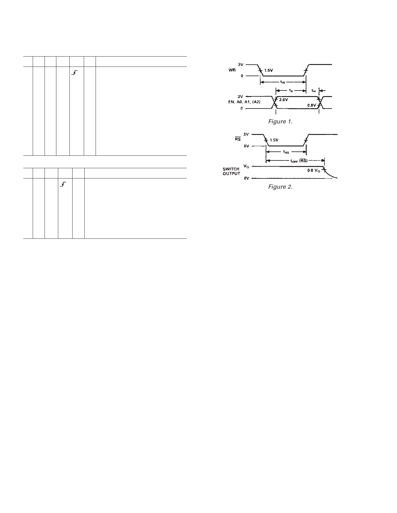
TIMING DIAGRAMS
Figure 1.
Figure 2.
Figure 1 shows the timing sequence for latching the switch
address and enable inputs. The latches are level sensitive; there-
fore, while WR is held low, the latches are transparent and the
switches respond to the address and enable inputs. This input
data is latched on the rising edge of WR.
Figure 2 shows the Reset Pulse Width, tRS, and Reset Turn-off
Time, tOFF (RS).
Note: All digital input signals rise and fall times measured from
10% to 90% of 3 V. tR = tF = 20 ns.
–6–
REV. B
Share Link: 