TC7MPN3125FTGEB 查看數據表(PDF) - Toshiba
零件编号
产品描述 (功能)
比赛名单
TC7MPN3125FTGEB Datasheet PDF : 22 Pages
| |||
TC7MPN3125FTG
TOSHIBA Digital Integrated Circuit Silicon Monolithic
TC7MPN3125FTG
Low Voltage/Low Power 2-Bit × 2 Dual Supply Bus Transceiver
The TC7MPN3125FTG is a dual supply, advanced high-speed
CMOS 4-bit dual supply voltage interface bus transceiver
fabricated with silicon gate CMOS technology.
It is also designed with over voltage tolerant inputs and
outputs up to 3.6 V.
Designed for use as an interface between a 1.2-V, 1.5-V, 1.8-V,
or 2.5-V bus and a 1.8-V, 2.5-V or 3.6-V bus in mixed 1.2-V, 1.5-V,
1.8-V or 2.5-V/1.8-V, 2.5-V or 3.6-V supply systems.
The A-port interfaces with the 1.2-V, 1.5-V, 1.8-V or 2.5-V bus,
the B-port with the 1.8-V, 2.5-V, 3.3-V bus.
The direction of data transmission is determined by the level of
Weight: 0.013 g (typ.)
the DIR input. The enable input ( OE ) can be used to disable the
device so that the buses are effectively isolated.
All inputs are equipped with protection circuits against static discharge or transient excess voltage.
Features
• Bidirectional interface between 1.2-V and 1.8-V, 1.2-V and 2.5-V, 1.2-V and 3.3-V, 1.5-V and 2.5-V, 1.5-V and
3.3-V, 1.8-V and 2.5-V, 1.8-V and 3.3-V or 2.5-V and 3.3-V buses.
• High-speed operation: tpd = 13.7 ns (max) (VCCA = 2.5 ± 0.2 V, VCCB = 3.3 ± 0.3 V)
tpd = 14.8 ns (max) (VCCA = 1.8 ± 0.15 V, VCCB = 3.3 ± 0.3 V)
tpd = 16.0 ns (max) (VCCA = 1.5 ± 0.1 V, VCCB = 3.3 ± 0.3 V)
tpd = 61 ns (max) (VCCA = 1.2 ± 0.1 V, VCCB = 3.3 ± 0.3 V)
tpd = 18.5 ns (max) (VCCA = 1.8 ± 0.15 V, VCCB = 2.5 ± 0.2 V)
tpd = 19.7 ns (max) (VCCA = 1.5 ± 0.15 V, VCCB = 2.5 ± 0.2 V)
tpd = 60 ns (max) (VCCA = 1.2 ± 0.15 V, VCCB = 2.5 ± 0.2 V)
tpd = 58 ns (max) (VCCA = 1.2 ± 0.1 V, VCCB = 1.8 ± 0.15 V)
• Output current: IOHB/IOLB = ±3 mA (min) (VCCB = 3.0 V)
IOHB/IOLB = ±2 mA (min) (VCCB = 2.3 V)
IOHB/IOLB = ±0.5 mA (min) (VCCB = 1.65 V)
IOHA/IOLA = ±9 mA (min) (VCCA = 2.3 V)
IOHA/IOLA = ±3 mA (min) (VCCA = 1.65 V)
IOHA/IOLA = ±1 mA (min) (VCCA = 1.4 V)
• Latch-up performance: ±300 mA
• ESD performance: Machine model ≥ ±200 V
Human body model ≥ ±2000 V
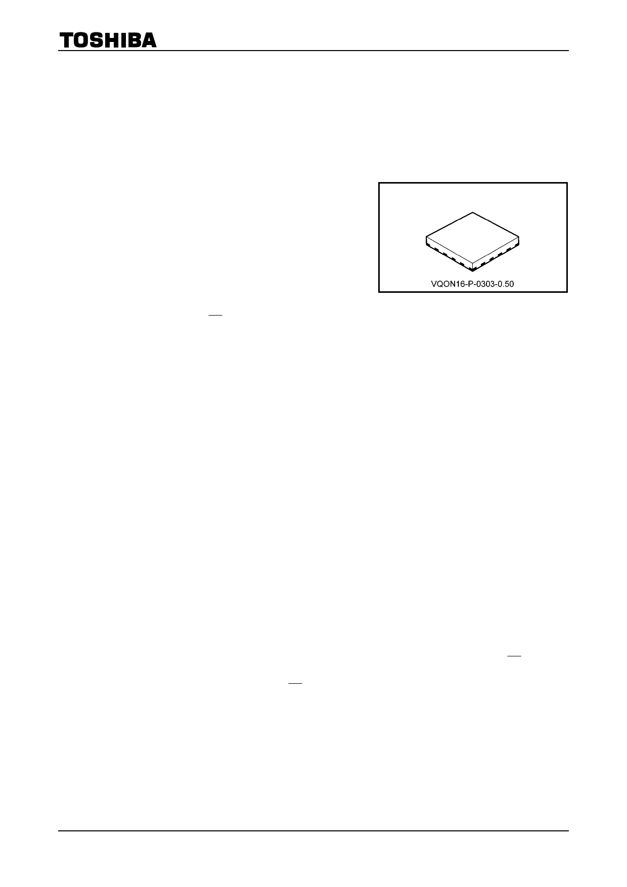
• Ultra-small package: VQON16
• Low current consumption: Using the new circuit significantly reduces current consumption when OE = “H”.
Suitable for battery-driven applications such as PDAs and cellular phones.
• Floating A-bus and B-bus are permitted. (when OE = “H”)
3.6-V tolerant function and power-down protection provided on all inputs and outputs.
Note 1: Do not apply a signal to any bus pins when it is in the output mode. Damage may result.
Note: When mounting VQON package, the type of recommended flux is RA or RMA.
1
2007-10-19
Share Link: 