AS1324 查看數據表(PDF) - austriamicrosystems AG
零件编号
产品描述 (功能)
比赛名单
AS1324 Datasheet PDF : 20 Pages
| |||
AS1324
Data Sheet - Application Information
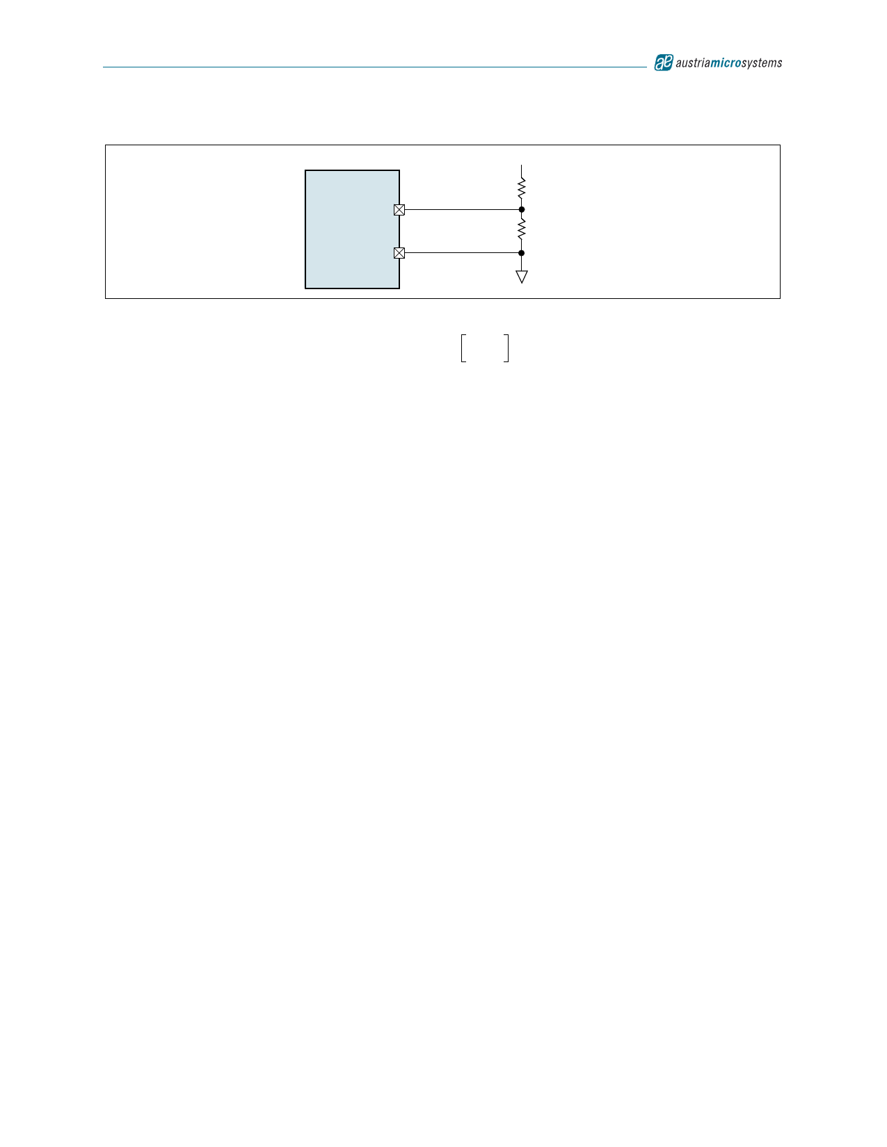
Figure 27. Setting the AS1324 Output Voltage
5
AS1324 VFB
2
GND
0.6V ≤ VOUT ≤ 5.5V
R2
R1<<R2
R1
Resistor values for the circuit shown in Figure 27 can be calculated as:
VOUT = 0,6 ×
1
+
R-----2-
R1
(EQ 7)
The output voltage can be adjusted by selecting different values for R1 and R2. For R1 a value between 10kΩ and
500kΩ is recommended. A higher resistance of R1 and R2 will result in a lower leakage current at the output. It is rec-
ommended to keep VIN 500mV higher than VOUT.
Efficiency
The efficiency of a switching regulator is equivalent to:
Efficiency = (POUT/PIN)100%
(EQ 8)
For optimum design, an analysis of the AS1324 is needed to determine efficiency limitations and to determine design
changes for improved efficiency. Efficiency can be expressed as:
Efficiency = 100% – (L1 + L2 + L3 + ...)
(EQ 9)
Where:
L1, L2, L3, etc. are the individual losses as a percentage of input power.
Althought all dissipative elements in the circuit produce losses, those four main sources should be considered for effi-
ciency calculation:
Input Voltage Quiescent Current Losses
The VIN current is the DC supply current given in the electrical characteristics which excludes MOSFET driver and con-
trol currents. VIN current results in a small (<0.1%) loss that increases with VIN, even at no load. The VIN quiescent cur-
rent loss dominates the efficiency loss at very low load currents.
I²R Losses
Most of the efficiency loss at medium to high load currents are attributed to I²R loss, and are calculated from the resis-
tances of the internal switches (RSW) and the external inductor (RL). In continuous mode, the average output current
flowing through inductor L is split between the internal switches. Therefore, the series resistance looking into the SW
pin is a function of both NMOS & PMOS RDS(ON) as well as the the duty cycle (DC) and can be calculated as follows:
RSW = (RDS(ON)PMOS)(DC) + (RDS(ON)NMOS)(1 – DC)
(EQ 10)
The RDS(ON) for both MOSFETs can be obtained from the Electrical Characteristics on page 4. Thus, to obtain I²R
losses calculate as follows:
I²R losses = IOUT²(RSW + RL)
(EQ 11)
Switching Losses
The switching current is the sum of the control currents and the MOSFET driver. The MOSFET driver current results
from switching the gate capacitance of the power MOSFETs. If a MOSFET gate is switched from low to high to low
again, a packet of charge dQ moves from VIN to ground. The resulting dQ/dt is a current out of VIN that is typically
much larger than the DC bias current. In continuous mode:
IGC = f(QPMOS + QNMOS)
(EQ 12)
Where: QPMOS and QNMOS are the gate charges of the internal MOSFET switches.
The losses of the gate charges are proportional to VIN and thus their effects will be more visible at higher supply volt-
ages.
Other Losses
www.austriamicrosystems.com
Revision 1.03
14 - 20
Share Link: 