AS1324 查看數據表(PDF) - austriamicrosystems AG
零件编号
产品描述 (功能)
比赛名单
AS1324 Datasheet PDF : 20 Pages
| |||
AS1324
Data Sheet - Pinout and Packaging
4 Pinout and Packaging
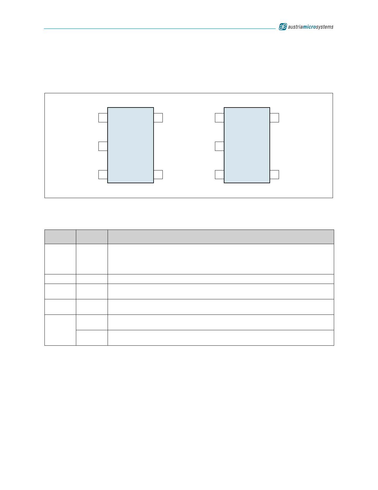
Pin Assignments
Figure 2. Pin Assignments (Top View)
EN 1
5 VFB
GND 2 AS1324
SW 3
4 VIN
EN 1
5 VOUT
AS1324-12/
GND 2 AS1324-15/
AS1324-18
SW 3
4 VIN
Pin Descriptions
Table 2. Pin Descriptions
Pin
Number
Pin Name
Description
Enable Input. Driving this pin above 1.5V enables the device. Driving this pin below 0.3V
puts the device in shutdown mode. In shutdown mode all functions are disabled while SW
1
EN
goes high impedance, drawing <1µA supply current.
Note: This pin should not be left floating.
2
GND Ground.
3
SW
Switch Node Connection to Inductor. This pin connects to the drains of the internal main
and synchronous power MOSFET switches.
Input Supply Voltage. This pin must be closely decoupled to GND with a ≥ 4.7µF ceramic
4
VIN capacitor. Connect to any supply voltage between 2.7 to 5.5V.
VFB
Feedback Pin. This pin receives the feedback voltage from the external resistor divider
across the output. (Adjustable voltage variant only.)
5
Output Voltage Feedback Pin. An internal resistor divider steps the output voltage down
VOUT for comparison to the internal reference voltage. (Fixed voltage variants only.)
www.austriamicrosystems.com
Revision 1.03
2 - 20
Share Link: 