AS1324 查看數據表(PDF) - austriamicrosystems AG
零件编号
产品描述 (功能)
比赛名单
AS1324 Datasheet PDF : 20 Pages
| |||
AS1324
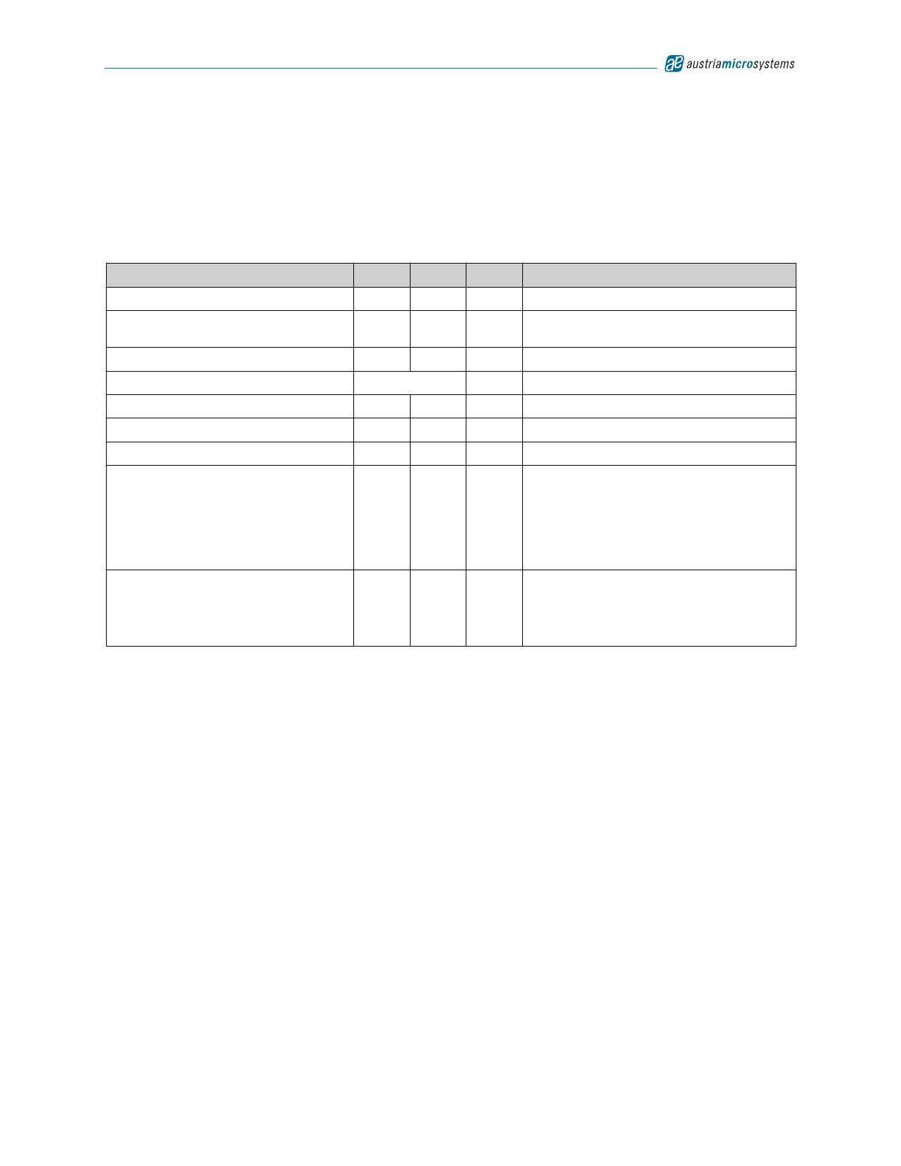
Data Sheet - Absolute Maximum Ratings
5 Absolute Maximum Ratings
Stresses beyond those listed in Table 3 may cause permanent damage to the device. These are stress ratings only,
and functional operation of the device at these or any other conditions beyond those indicated in Section 6 Electrical
Characteristics on page 4 is not implied. Exposure to absolute maximum rating conditions for extended periods may
affect device reliability.
Table 3. Absolute Maximum Ratings
Parameter
VIN to GND
Min Max Units
-0.3
7
V
Comments
SW, EN, FB to GND
Thermal Resistance ΘJA
ESD
Latch-Up
-0.3
VIN
+ 0.3
207.4
2
-100 +100
V
ºC/W
kV
mA
on PCB
HBM MIL-Std. 883E 3015.7 methods
JEDEC 78
Operating Temperature Range
-40
+85
ºC
Storage Temperature Range
-65
+125
ºC
Package Body Temperature
Junction Temperature
+260
125
The reflow peak soldering temperature (body
temperature) specified is in accordance with
IPC/JEDEC J-STD-020C “Moisture/Reflow
ºC
Sensitivity Classification for Non-Hermetic
Solid State Surface Mount Devices”.
The lead finish for Pb-free leaded packages
is matte tin (100% Sn).
Junction temperature (TJ) is calculated from
the ambient temperature (TAMB) and power
ºC dissipation (PD) as:
TJ = TAMB + (PD)(207.4ºC/W) (EQ 1)
www.austriamicrosystems.com
Revision 1.03
3 - 20
Share Link: 