CL7128E 查看數據表(PDF) - Clear Logic
零件编号
产品描述 (功能)
比赛名单
CL7128E Datasheet PDF : 16 Pages
| |||
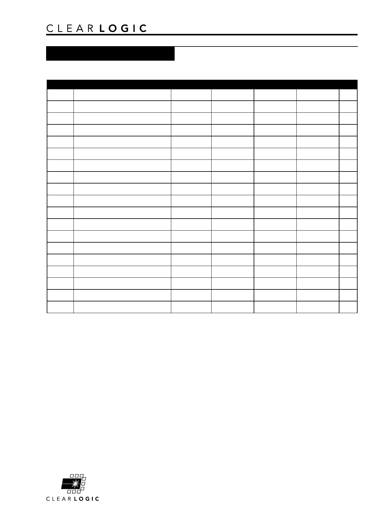
CL7128E and CL7128S Laser Processed Logic Devices
AC Electrical Specifications
I/O Element Timing Parameters
Speed: -5
Symbol
Parameter
Conditions Min Max
tPD1 Input to non-registered output
CL = 35 pF
5.0
tPD2 I/O input to non-registered output
CL = 35 pF
5.0
tSU Global clock setup time
2.9
tH
Global clock hold time
0.0
tFSU Global clock setup time of fast input
2.5
tFH Global clock hold time of fast input
0.0
tCO1 Global clock to output delay
CL = 35 pF
3.2
tCH Global clock high time
2.0
tCL Global clock low time
2.0
tASU Array clock setup time
0.7
tAH Array clock hold time
1.8
tACO1 Array clock to output delay
CL = 35 pF
5.4
tACH Array clock high time
2.5
tACL Array clock low time
2.5
tODH Output data hold time after clock
CL = 35 pF
1.0
tCNT Minimum global clock period
5.7
fCNT Max. internal global clock frequency
175.4
tACNT Minimum array clock period
5.5
fACNT Max. internal array clock frequency
175.4
Speed: -6
Min Max
6.0
6.0
3.4
0.0
2.5
0.0
4.0
3.0
3.0
0.9
1.8
6.5
3.0
3.0
1.0
6.8
147.1
6.8
147.1
Speed: -7
Min Max Unit
7.5 ns
7.5 ns
6.0
ns
0.0
ns
3.0
ns
0.5
ns
4.5 ns
3.0
ns
3.0
ns
3.0
ns
2.0
ns
7.5 ns
3.0
ns
3.0
ns
1.0
ns
8.0 ns
125.0
MHz
8.0 ns
125.0
MHz
7K tbl 06B1
Page 7
Share Link: 