IRFP350 查看數據表(PDF) - Intersil
零件编号
产品描述 (功能)
比赛名单
IRFP350 Datasheet PDF : 7 Pages
| |||
IRFP350
Absolute Maximum Ratings TC = 25oC, Unless Otherwise Specified
Drain to Source Voltage (Note 1) . . . . . . . . . . . . . . . . . . . . . . . . . . . . . . . . . . . . . . . . . . . . . . . . . . . . . . .VDS
Drain to Gate Voltage (RGS = 20kΩ) (Note 1) . . . . . . . . . . . . . . . . . . . . . . . . . . . . . . . . . . . . . . . . . . . VDGR
Continuous Drain Current . . . . . . . . . . . . . . . . . . . . . . . . . . . . . . . . . . . . . . . . . . . . . . . . . . . . . . . . . . . . . ID
TC = 100oC. . . . . . . . . . . . . . . . . . . . . . . . . . . . . . . . . . . . . . . . . . . . . . . . . . . . . . . . . . . . . . . . . . . . . ID
Pulsed Drain Current (Note 3) . . . . . . . . . . . . . . . . . . . . . . . . . . . . . . . . . . . . . . . . . . . . . . . . . . . . . . . . . IDM
Gate to Source Voltage . . . . . . . . . . . . . . . . . . . . . . . . . . . . . . . . . . . . . . . . . . . . . . . . . . . . . . . . . . . . . .VGS
Maximum Power Dissipation . . . . . . . . . . . . . . . . . . . . . . . . . . . . . . . . . . . . . . . . . . . . . . . . . . . . . . . . . . .PD
Linear Derating Factor . . . . . . . . . . . . . . . . . . . . . . . . . . . . . . . . . . . . . . . . . . . . . . . . . . . . . . . . . . . . . . . .
Single Pulse Avalanche Energy Rating (Note 4) . . . . . . . . . . . . . . . . . . . . . . . . . . . . . . . . . . . . . . . . . . .EAS
Operating and Storage Temperature . . . . . . . . . . . . . . . . . . . . . . . . . . . . . . . . . . . . . . . . . . . . . . . TJ, TSTG
Maximum Temperature for Soldering
Leads at 0.063in (1.6mm) from Case for 10s. . . . . . . . . . . . . . . . . . . . . . . . . . . . . . . . . . . . . . . . . . . . . TL
Package Body for 10s, See Techbrief 334 . . . . . . . . . . . . . . . . . . . . . . . . . . . . . . . . . . . . . . . . . . . . . Tpkg
IRFP350
400
400
16
10
64
±20
180
1.44
700
-55 to 150
300
260
UNITS
V
V
A
A
A
V
W
W/oC
mJ
oC
oC
oC
CAUTION: Stresses above those listed in “Absolute Maximum Ratings” may cause permanent damage to the device. This is a stress only rating and operation of the
device at these or any other conditions above those indicated in the operational sections of this specification is not implied.
NOTE:
1. TJ = 25oC to 125oC.
Electrical Specifications TC = 25oC, Unless Otherwise Specified
PARAMETER
SYMBOL
TEST CONDITIONS
MIN TYP MAX UNITS
Drain to Source Breakdown Voltage
BVDSS VGS = 0V, ID = 250µA (Figure 10)
400
-
-
V
Gate to Threshold Voltage
VGS(TH) VGS = VDS, ID = 250µA
2.0
-
4.0
V
Zero-Gate Voltage Drain Current
IDSS VDS = Rated BVDSS, VGS = 0V
-
-
25
µA
VDS = 0.8 x Rated BVDSS, VGS = 0V, TJ = 125oC
-
-
250
µA
On-State Drain Current (Note 2)
ID(ON) VDS > ID(ON) x rDS(ON)MAX, VGS = 10V (Figure 7)
16
-
-
A
Gate to Source Leakage Current
IGSS VGS = ±20V
-
-
±100
nA
Drain to Source On Resistance (Note 2) rDS(ON) VGS = 10V, ID = 8.9A (Figures 8, 9)
- 0.250 0.300
Ω
Forward Transconductance (Note 2)
gfs
VDS = 2 x VGS, ID = 8.0A (Figure 12)
8.0
10
-
S
Turn-On Delay Time
Rise Time
Turn-Off Delay Time
tD(ON)
tr
tD(OFF)
VDD = 200V, ID = 16A, RGS = 6.2Ω, VGS = 10V,
RL = 12.3Ω
MOSFET Switching Times are Essentially
Independent of Operating Temperature
-
12
18
ns
-
51
77
ns
-
75 110
ns
Fall Time
tf
-
47
71
ns
Total Gate Charge
(Gate to Source + Gate to Drain)
Gate to Source Charge
Gate to Drain “Miller” Charge
Qg
VGS = 10V, ID = 16A, VDS = 0.8 x Rated BVDSS.
-
IG(REF) = 1.5mA (Figure 14)
Qgs
Gate Charge is Essentially Independent of Operating
Temperature
-
Qgd
-
87 130
nC
10
-
nC
33
-
nC
Input Capacitance
CISS VGS = 0V, VDS = 25V, f = 1.0MHz (Figure 11)
-
2000
-
pF
Output Capacitance
COSS
-
400
-
pF
Reverse-Transfer Capacitance
CRSS
-
100
-
pF
Internal Drain Inductance
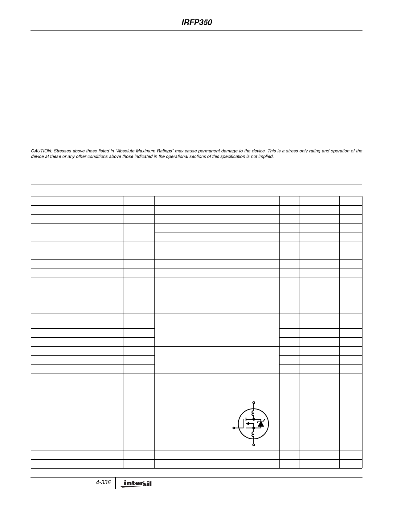
LD
Measured Between the Modified MOSFET
Contact Screw on Header Symbol Showing the
that is Closer to Source Internal Devices
and Gate Pins and Center Inductances
of Die
D
-
5.0
-
nH
Internal Source Inductance
LS
Measured from the
LD
Source Lead, 6mm
(0.25in) From Header to
G
Source Bonding Pad
LS
-
12.5
-
nH
Junction to Case
Junction to Ambient
RθJC
RθJA
Free Air Operation
S
-
-
0.70 oC/W
-
-
30
oC/W
4-336
Share Link: 