CXP508L4 查看數據表(PDF) - Sony Semiconductor
零件编号
产品描述 (功能)
比赛名单
CXP508L4 Datasheet PDF : 11 Pages
| |||
CXP508L4/508L6
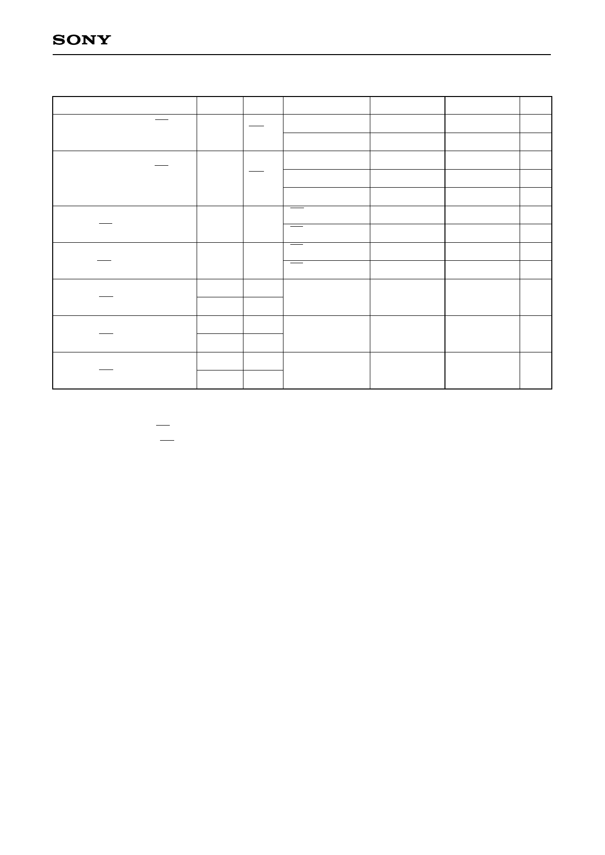
(2) Serial transfer
Item
Serial transfer clock (SC)
cycle time
Symbol Pin
tKCY
SC
Serial transfer clock (SC)
high and low level widths
tKH
tKL
SC
Serial data input setup time
(against SC ↑)
tSIK
Serial data input hold time
(against SC ↑)
tKSI
High data∗3 output delay time
from the SC falling time
High data∗4 output delay time
from the SC falling time
Low data output delay time
from the SC falling time
tKSOA
tKSOB
tKSOA
tKSOB
tKSOA
tKSOB
SI
SI
SOA
SOB
SOA
SOB
SOA
SOB
(Ta = –20 to +75°C, VDD = 2.4 to 3.5V, VSS = 0V)
Condition
Min.
Max.
Unit
Input mode
tsys/4 + 1.42
µs
Output mode
tsys
µs
input mode
tsys/8 + 0.7
µs
Output mode∗1 tsys/2 – 0.1
µs
Output mode∗2 tsys/2 – 1.6
µs
SC input mode
0.1
µs
SC output mode
0.2
µs
SC input mode tsys/8 + 0.5
µs
SC output mode
0.1
µs
tsys/8 + 0.5 µs
tsys/8 + 1.6 µs
tsys/8 + 0.5 µs
Note 1) tsys = 8/fc
Note 2) The load of data output delay time is 50pF + 1TTL.
∗1 It is specified when SC pin is selected to the 3-atate output by the mask option.
∗2 It is specified when SC pin is selected to the pull-up resistance by the mask option. As the tsys receives
restriction by this item, take notice that it limits the upper limit of the system clock frequency fc.
∗3 It is specified when SOA and PX1/SOB pins are selected to the 3-state output by the mask option.
∗4 It is specified when SOA and PX1/SOB pins are selected to the pull-up resistance by the mask option.
–7–
Share Link: 