CXP5078 查看數據表(PDF) - Sony Semiconductor
零件编号
产品描述 (功能)
比赛名单
CXP5078 Datasheet PDF : 18 Pages
| |||
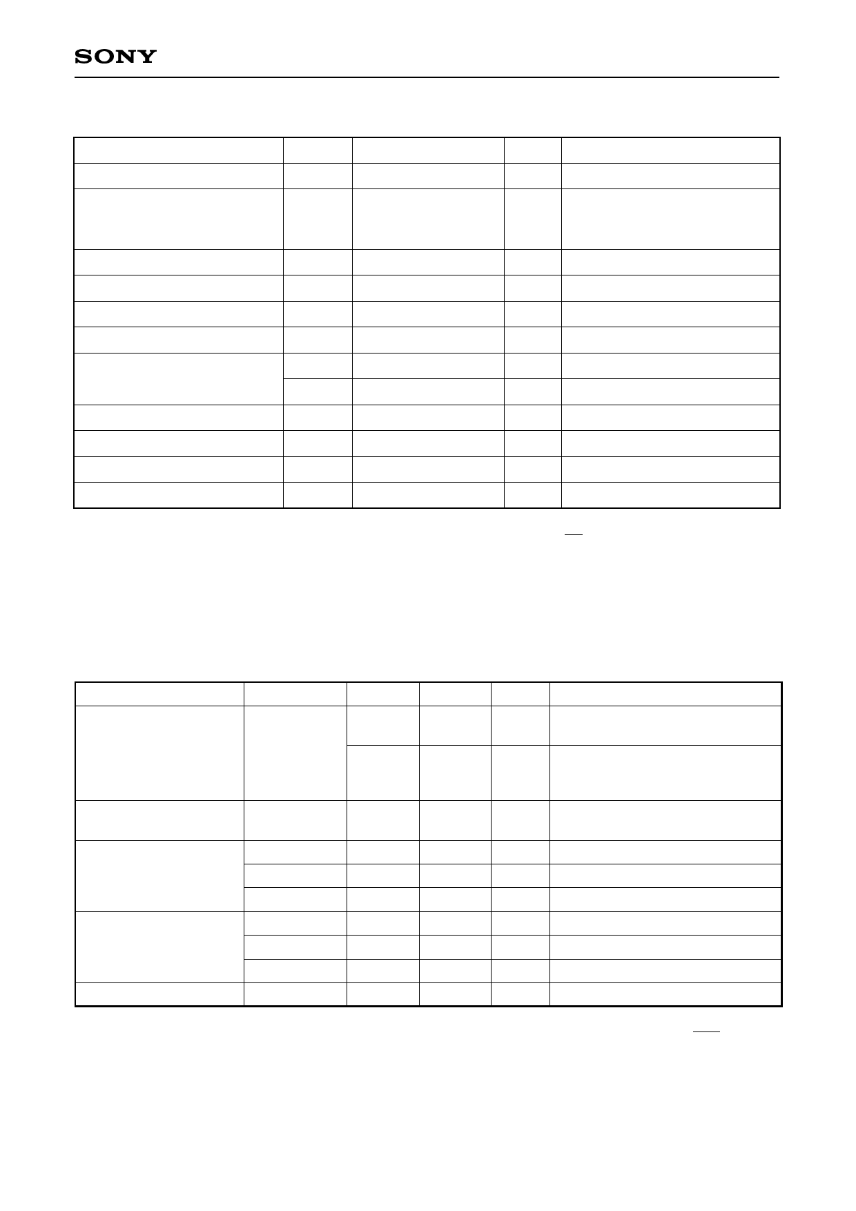
CXP5076/5078
Absolute Maximum Ratings
(Ta = –20 to +75°C, VSS = 0V)
Item
Symbol
Rating
Unit
Remarks
Power supply voltage
VDD
–0.3 to +7.0
V
LCD bias voltage
Input voltage
Output voltage
High level output current
VCL1,
VCL2,
VCL3
VIN
VOUT
IOH
–0.3 to +7.0∗1
–0.3 to +7.0∗1
–0.3 to +7.0∗1
–5
V
V
V
mA General purpose port∗2: per pin
High level total output current
Low level output current
∑IOH
IOL
IOLC
–50
mA Entire pins total
15
mA General purpose port∗2: per pin
20
mA High current port∗3: per pin
Low level total output current ∑IOL
100
mA Entire pins total
Operating temperature
Topr
–20 to +75
°C
Storage tamperature
Tstg
–55 to +150
°C
Allowable power dissipation PD
600
mW
∗1 VLC1, VLC2, VLC3, VIN and VOUT should not exceed VDD + 0.3V.
∗2 Specifies the output current of the general purpose I/O port PA to PI, SO, SC, PY0 and PY1.
∗3 The high current operation transistors are the N-ch transistors of the PC and PD ports.
Note) Usage exceeding absolute maximum ratings may permanently impair the LSI. Normal operation should
better take place under the recommended operation conditions. Exceeding those conditions may
adversely affect the reliability of the LSI.
Recommended Operating Condition
(Vss = 0V)
Item
Symbol
Min.
Max. Unit
Remarks
4.5
5.5
V
Guaranteed range of operation by
EXTAL clock
Power supply voltage VDD
Guaranteed range of operation by
2.5
5.5
V TEX clock, guaranteed range of
data hold during STOP.
LCD bias voltage
VCL1, VCL2,
VCL3
VSS
VDD
V Liquid crystal power supply range∗1
High level input voltage
VIH
VIHS
VIHEX
0.7VDD
VDD
V
0.8VDD
VDD
V Hysteresis input∗2
VDD – 0.4 VDD + 0.3
V
EXTAL pin∗3
Low level input voltage
VIL
VILS
VILEX
0
0
–0.3
0.3VDD
0.2VDD
0.4
V
V Hysteresis input∗2
V EXTAL pin∗3
Operating temperature Topr
–20
+75
°C
∗1 The optimum value is determined by the characteristics of the liquid crystal display element used.
∗2 The TEX pin when the counter mode is selected by each of INT, RMC, PX0, PX2, PY2, PY3, RST pins and
mask option.
∗3 Specified only during external clock input.
–9–
Share Link: 