W42C32-05M 查看數據表(PDF) - Cypress Semiconductor
零件编号
产品描述 (功能)
比赛名单
W42C32-05M Datasheet PDF : 8 Pages
| |||

W42C32-05M
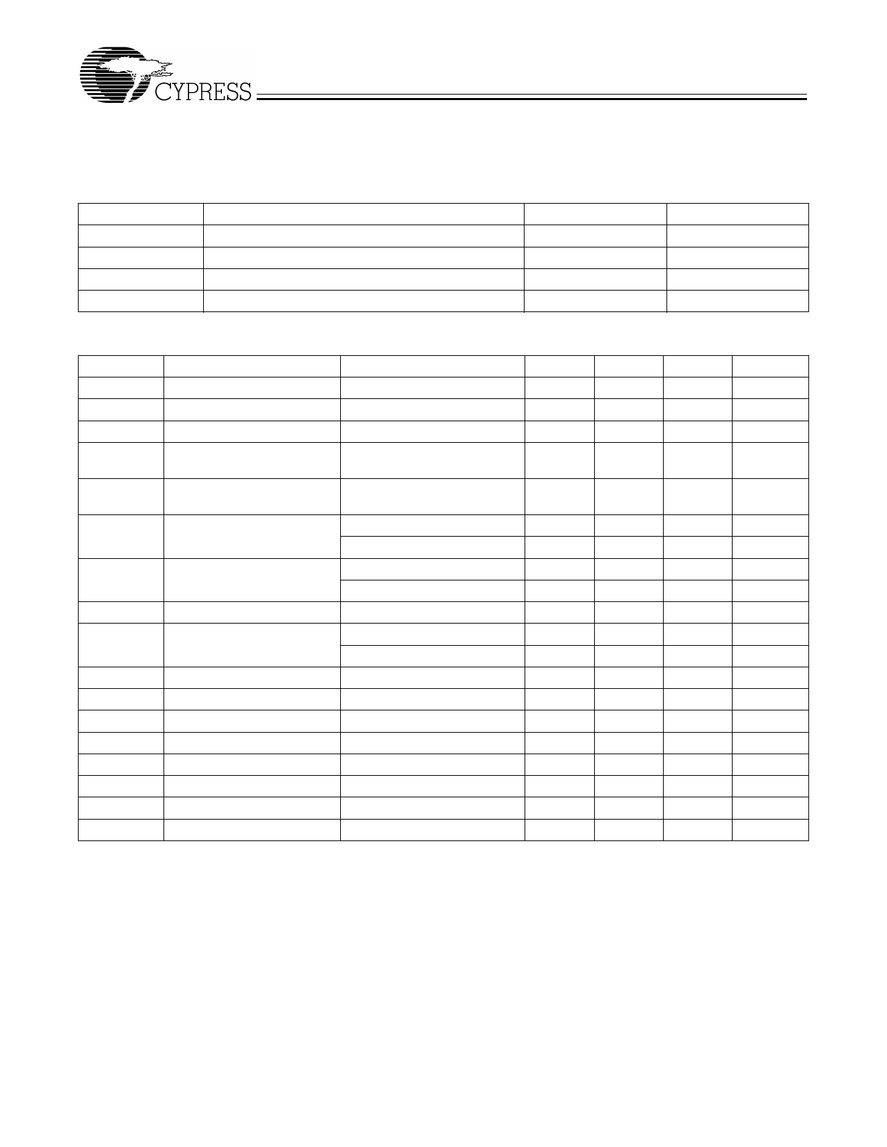
Absolute Maximum Ratings
Stresses greater than those listed in this table may cause per-
manent damage to the device. These represent a stress rating
only. Operation of the device at these or any other conditions
above those specified in the operating sections of this specifi-
cation is not implied. Maximum conditions for extended peri-
ods may affect reliability.
Parameter
VDD, VIN
TSTG
TA
TB
Description
Voltage on any pin with respect to GND
Storage Temperature
Operating Temperature
Ambient Temperature under Bias
Rating
Unit
–0.5 to +7.0
V
–65 to +150
°C
0 to +70
°C
–55 to +125
°C
DC Electrical Characteristics: 0°C < TA < 70°C, VDD = 5.0V±10%, 3.3V±5%
Parameter
Description
Test Condition
Min.
IDD
Supply Current
VDD = 5.0V
IPD
Power Down Supply Current VDD = 5.0V
tOFF
Power Down Time
tON
Power Up Time
First locked clock cycle after
PD# goes HIGH
tEN
Enable/Disable Time
Time required for output to be
enabled/disabled
VIL
Input Low Voltage
VDD = 5.0V
VDD = 3.3V
VIH
Input High Voltage
VDD = 5.0V
VDD = 3.3V
VOL
Output Low Voltage
VOH
Output High Voltage
VDD = 5.0V
VDD = 3.3V
IIL
Input Low Current
IIH
Input High Current
IOL
Output Low Current
@ 0.4V, VDD = 3.3V
IOH
Output High Current
@ 2.4V, VDD = 3.3V
CI
Input Capacitance
All pins except X1, X2
CL
XTAL Load Capacitance
Pins X1, X2
RP
Input Pull-Up Resistor
VIN = 0V
ZOUT
Clock Output Impedance
Any clock output pin
Note:
3. Cycle refers to input clock cycles supplied by the input crystal or reference.
3.0
0.7VDD
2.4
2.4
Typ.
35
2.4
2.4
300
33
Max.
45
75
4
5
4
Unit
mA
µA
cycles[3]
ms
cycles[3]
0.8
V
0.15VDD
V
V
V
0.4
V
V
V
–100
µA
10
µA
mA
mA
7
pF
16
pF
kΩ
Ω
5