2115M-1.2G1 查看數據表(PDF) - BCD Semiconductor
零件编号
产品描述 (功能)
比赛名单
2115M-1.2G1 Datasheet PDF : 19 Pages
| |||
Preliminary Datasheet
1A LOW NOISE CMOS LDO REGULATOR WITH ENABLE AP2115
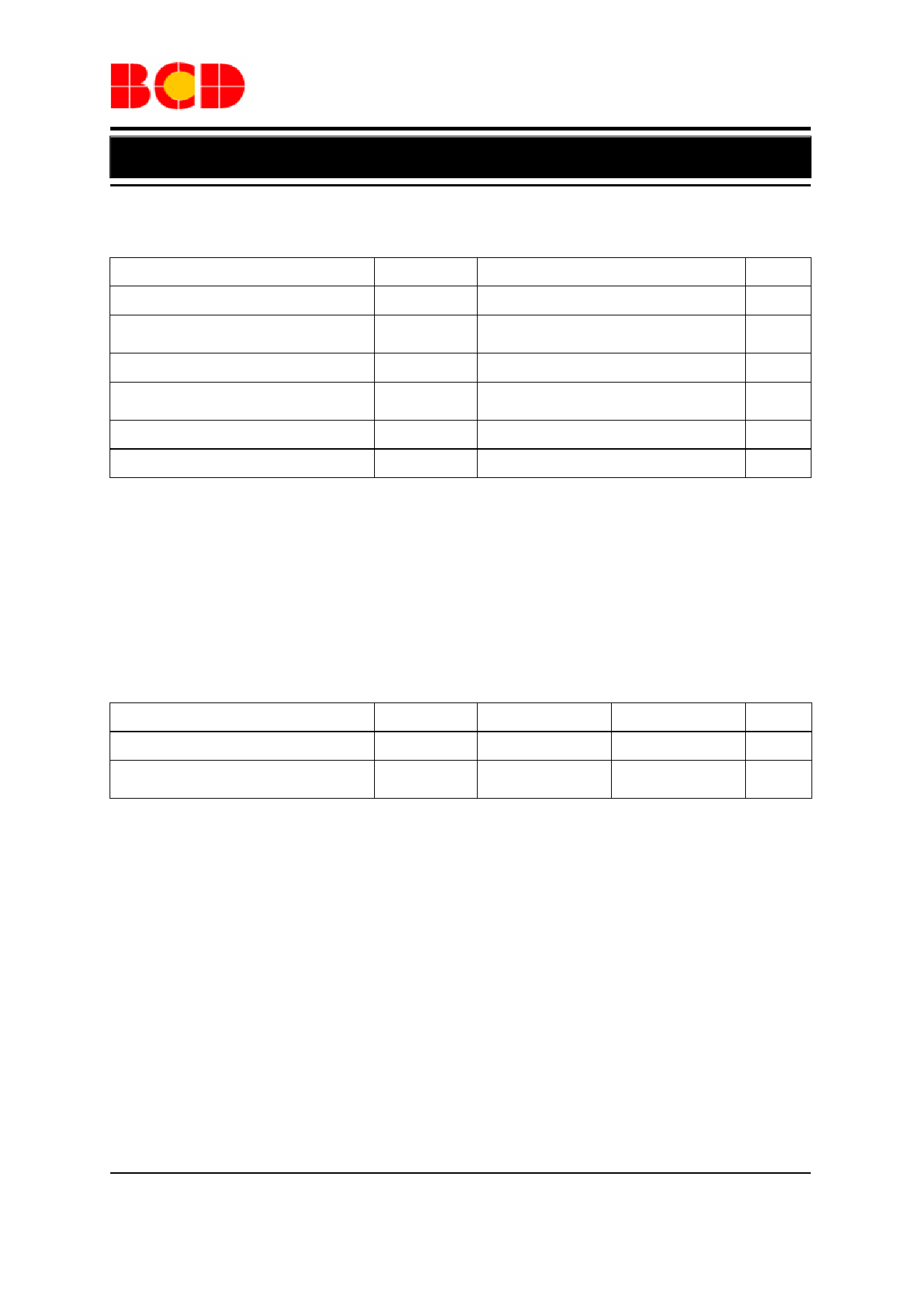
Absolute Maximum Ratings (Note 1)
Parameter
Power Supply Voltage
Operating Junction Temperature
Range
Storage temperature Range
Lead Temperature (Soldering,10
Seconds)
ESD (Machine Model)
ESD (Human Body Model)
Symbol
VCC
TJ
TSTG
TLEAD
Value
6.5
150
-65 to 150
260
400
4000
Unit
V
ºC
ºC
ºC
V
V
Note 1: Stresses greater than those listed under “Absolute Maximum Ratings” may cause permanent damage to
the device. These are stress ratings only, and functional operation of the device at these or any other conditions
beyond those indicated under “Recommended Operating Conditions” is not implied. Exposure to “Absolute
Maximum Ratings” for extended periods may affect device reliability.
Recommended Operating Conditions
Parameter
Symbol
Min
Supply Voltage
VIN
2.5
Ambient Operation Temperature
Range
TA
-40
Max
6.0
85
Unit
V
°C
Jul. 2011 Rev 1. 1
BCD Semiconductor Manufacturing Limited
5
Share Link: 