SPT7935 查看數據表(PDF) - Cadeka Microcircuits LLC.
零件编号
产品描述 (功能)
比赛名单
SPT7935 Datasheet PDF : 8 Pages
| |||

The AC coupled input is most conveniently implemented
using a transformer with a center tapped secondary winding.
The center tap is connected to the VCM pin as shown in
figure 2. To obtain low distortion, it is important that the
selected transformer does not exhibit core saturation at the
full-scale voltage. Proper termination of the input is important
for input signal purity. A small capacitor across the inputs
attenuates kickback noise from the internal sample and hold.
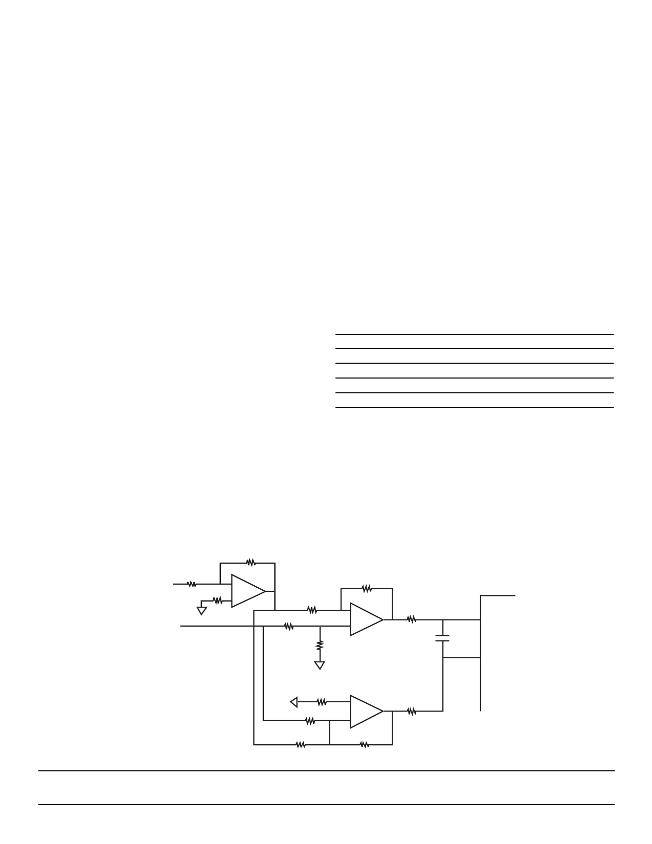
Figure 3 illustrates a solution (based on operational amplifi-
ers) that can be used if a DC coupled single-ended input is
desired. The selection criteria of the buffer op-amps is as
follows:
– Open loop gain >75 dB
– Gain bandwidth product >50 MHz
– Total harmonic distortion ≤–75 dB
– Signal to noise ratio >75 dB
POWER SUPPLIES AND GROUNDING
The SPT7935 is operated from a single power supply in the
range of 2.8 to 3.6 volts. Nominal operation is suggested to
be 3.3 volts. All power supply pins should be bypassed as
close to the package as possible. The analog and digital
grounds should be connected together with a ferrite bead as
shown in the typical interface circuit and as close to the ADC
as possible.
REFERENCES
The SPT7935 has a differential analog input. The voltages
applied to the VREF+ and VREF- pins determine the input
voltage range and are equal to ±(VREF+ – VREF–). This
voltage range will be symmetric about the common mode
voltage. Externally generated reference voltages must be
connected to these pins. (See figure 2, Typical Interface
Circuit.) For best performance, these voltages should be
symmetrical about the midpoint of the supply voltage.
COMMON MODE VOLTAGE
REFERENCE CIRCUIT
The SPT7935 has an on-board common mode voltage refer-
ence circuit (VCM). It is typically one-half of the supply voltage
and can drive loads of up to 20 µA. This circuit is commonly
used to drive the center tap of the RF transformer in fully
differential applications. For single-ended applications, this
output can be used to provide the level shifting required for
the single-to-differential converter conversion circuit.
BIAS CURRENT CIRCUITS
The bias currents suggested (Bias 1 and Bias 2 in figure 2)
optimize device performance for the stated sample rate of
20 MSPS. To achieve the best dynamic performance when
operating the device at sample rates other than 20 MSPS, the
bias current levels should be adjusted. Table I shows the
settings for Bias 1 and Bias 2 for selected sample rates. The
“Bias Voltage vs Bias Current” graphs on page 4 show the
relationship between the bias current and the bias voltage.
Table I – Sample Rate Settings
Sample Rate (MHz)
1
5
10
20
Bias 1 (µA)
20
50
80
90
Bias 2 (µA)
3.5
6.5
8.0
9.5
Figure 3 – DC-Coupled Single Ended to Differential Conversion (Power Supplies and Bypassing are Not Shown)
R3
VCM
R3
–
+
Input
Voltage
(±0.5 V)
(R3)/2
R
R2
R2
R
–
51 Ω
+
15 pF
ADC
VIN+
VIN–
51 Ω
+
R
–
R
R
51 Ω
SPT7935
6
7/12/00