SPT7935 查看數據表(PDF) - Cadeka Microcircuits LLC.
零件编号
产品描述 (功能)
比赛名单
SPT7935 Datasheet PDF : 8 Pages
| |||
CLOCK
The SPT7935 accepts a low voltage CMOS logic level at
the CLK input. The duty cycle of the clock should be kept as
close to 50% as possible. Because consecutive stages in the
ADC are clocked in opposite phase to each other, a non-50%
duty cycle reduces the settling time available for every other
stage and thus potentially causing a degradation of dynamic
performance.
For optimal performance at high input frequencies, the clock
should have low jitter and fast edges. The rise/fall times
should be kept shorter than 2 ns. Overshoot and undershoot
should be avoided. Clock jitter causes the noise floor to rise
proportional to the input frequency. Because jitter can be
caused by crosstalk on the PC board, it is recommended that
the clock trace be kept as short as possible and standard
transmission line practices be followed.
DIGITAL OUTPUTS
The digital output data appears in an offset binary code at
3.3 V CMOS logic levels. A negative full scale input results in
an all zeros output code (000…0). A positive full scale input
results in an all 1’s code (111…1). The output data is available
7.5 clock cycles after the data is sampled. The input signal is
sampled on the high to low transition of the input clock. Output
data should be latched on the low to high clock transition as
shown in figure 1, the Timing Diagram. The output data is
invalid for the first 20 clock cycles after the device is powered up.
EVALUATION BOARD
The EB7935 Evaluation Board is available to aid designers in
demonstrating the full performance capability of the
SPT7935. The board includes an on-board clock driver,
adjustable voltage references, adjustable bias current cir-
cuits, single-to-differential input buffers with adjustable lev-
els, a single-to-differential transformer (1:1), digital output
buffers and 3.3/5 V adjustable logic outputs. An application
note (AN7935) is also available which describes the opera-
tion of the evaluation board and provides an example of the
recommended power and ground layout and signal routing.
Contact the factory for price and availability.
A
B
Index
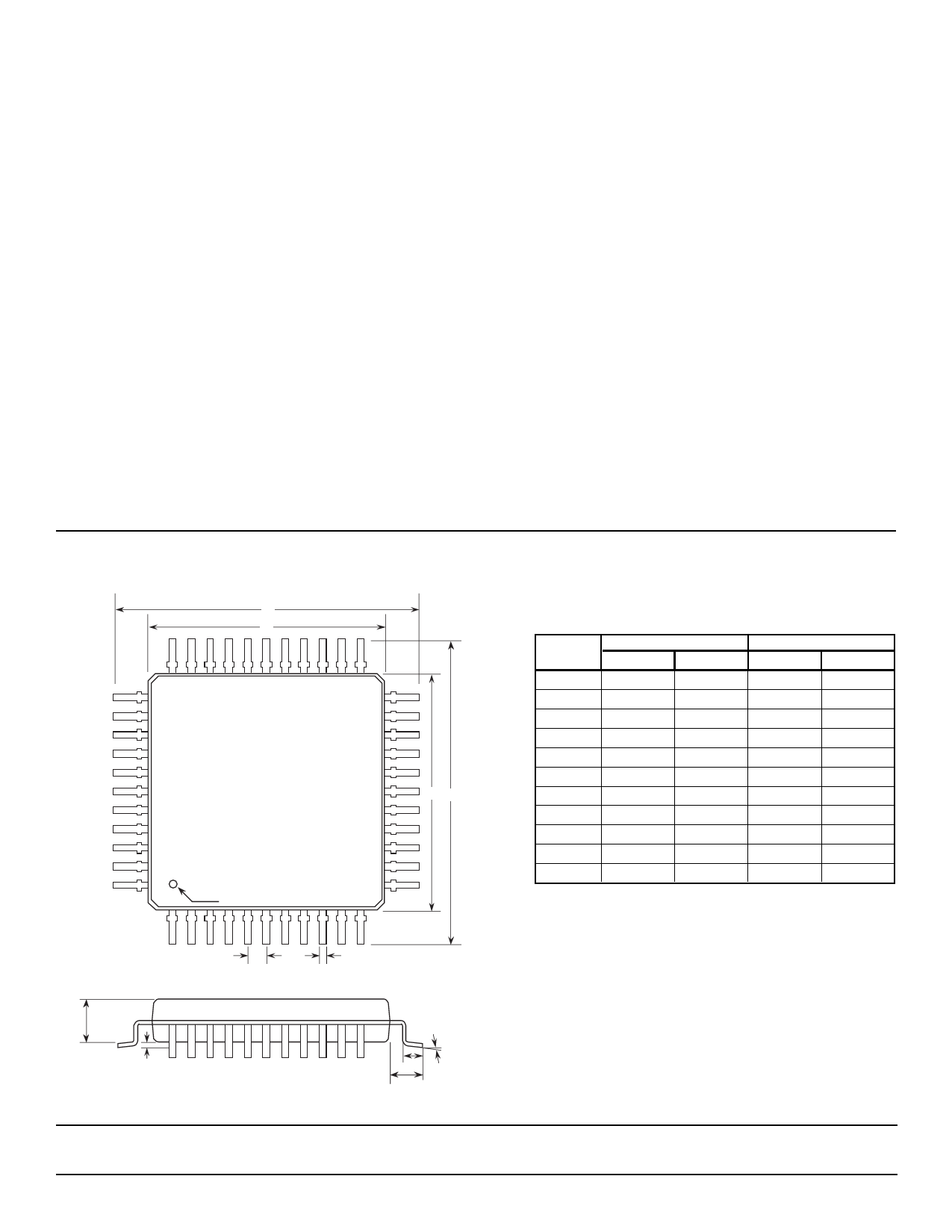
PACKAGE OUTLINE
44L TQFP
CD
INCHES
SYMBOL MIN
MAX
A
0.472 Typ
B
0.394 Typ
C
0.394 Typ
D
0.472 Typ
E
0.031 Typ
F
0.012
0.018
G
0.053
0.057
H
0.002
0.006
I
0.018
0.030
J
0.039 Typ
K
0-7°
MILLIMETERS
MIN
MAX
12.00 Typ
10.00 Typ
10.00 Typ
12.00 Typ
0.80 Typ
0.300
0.45
1.35
1.45
0.05
0.15
0.450
0.750
1.00 Typ
0-7°
Pin 1
E
F
G
H
K
I
J
7
SPT7935
7/12/00
Share Link: 