UT62V25716BS-70LL 查看數據表(PDF) - Utron Technology Inc
零件编号
产品描述 (功能)
比赛名单
UT62V25716BS-70LL Datasheet PDF : 10 Pages
| |||
Rev. 1.0
UTRON
UT62V25716
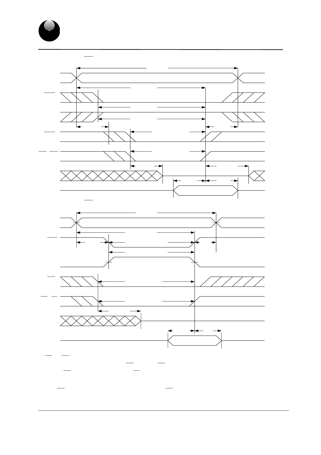
256K X 16 BIT LOW POWER CMOS SRAM
WRITE CYCLE 1 ( WE Controlled) (1,2,3,5)
t WC
Address
CE1
CE2
t AS
WE
t AW
t CW1
t CW2
t WP
t WR
LB , UB
Dout
Din
t PWB
t WH
(4)
High-Z
t DW
t OW
(4)
t DH
Data Valid
WRITE CYCLE 2 ( CE1and CE2 Controlled) (1,2,5)
t WC
Address
CE1
t AS
CE2
t AW
t CW1
t CW2
t WR
WE
t WP
LB , UB
t PWB
Dout
t WHZ
High-Z
t DW
t DH
Din
Data Valid
Notes :
1. WE or CE1 must be HIGH during all address transitions.
2. A write occurs during the overlap of a low CE1 and a low WE .
3. During a WE controlled with write cycle with OE LOW, tWP must be greater than tWHZ+tDW to allow the drivers to turn off and
data to be placed on the bus.
4. During this period, I/O pins are in the output state, and input singals must not be applied.
5. If the CE1 LOW transition occurs simultaneously with or after WE LOW transition, the outputs remain in a high impedance
state.
6. tOW and tWHZ are specified with CL = 5pF. Transition is measured ± 500mV from steady state.
UTRON TECHNOLOGY INC.
1F, No. 11, R&D Rd. II, Science-Based Industrial Park, Hsinchu, Taiwan, R. O. C.
TEL: 886-3-5777882 FAX: 886-3-5777919
5
P80065
Share Link: 