RP102N331D-TR 查看數據表(PDF) - RICOH Co.,Ltd.
零件编号
产品描述 (功能)
比赛名单
RP102N331D-TR Datasheet PDF : 30 Pages
| |||
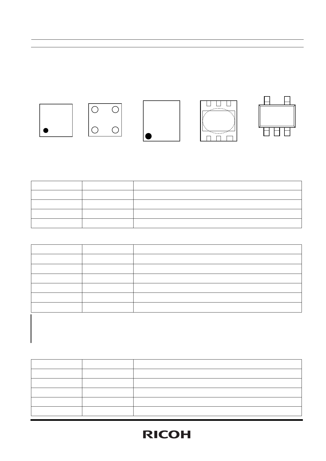
PIN CONFIGURATIONS
WLCSP-4-P2
Mark Side
Bump Side
2
2
1
A
B
1
B
A
RP102x
NO.EA-141-160705
DFN(PLP)1820-6
Top View
654
Bottom View
456
1
123
321
SOT-23-5
5
4
(mark side)
123
PIN DESCRIPTION
WLCSP-4-P2
Pin No
A1
A2
B1
B2
Symbol
VDD
VOUT
CE
GND
Pin Description
Input Pin
Output Pin
Chip Enable Pin ("H" Active)
Ground Pin
DFN(PLP)1820-6
Pin No
Symbol
Pin Description
1
VOUT
Output Pin2
2
VOUT
Output Pin2
3
GND
Ground Pin
4
CE
Chip Enable Pin ("H" Active)
5
VDD
Input Pin2
6
VDD
Input Pin2
1) Tab is GND level. (They are connected to the reverse side of this IC.)
The tab is better to be connected to the GND, but leaving it open is also acceptable.
2) No.1 pin and No.2 pin, No.5 pin and No.6 pin of DFN(PLP)1820-6 package must be wired when it is
mounted on board.
SOT-23-5
Pin No
1
2
3
4
5
Symbol
VDD
GND
CE
NC
VOUT
Pin Description
Input Pin
Ground Pin
Chip Enable Pin ("H" Active)
No Connection
Output Pin
3
Share Link: 