CL8452A 查看數據表(PDF) - Clear Logic
零件编号
产品描述 (功能)
比赛名单
CL8452A Datasheet PDF : 12 Pages
| |||
CL8452A Laser-Configured ASIC
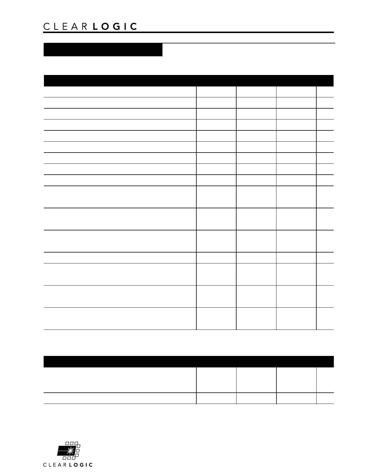
AC Electrical Specifications
I/O Element Timing Parameters [5]
Symbol
Parameter
Conditions
Speed: -2
Speed: -3
Speed: -4
Min Max Min Max Min Max Unit
tIOD IOE register data delay
tIOC IOE register control signal delay
tIOE Output enable delay
tIOCO IOE register clock to output delay
tIOCOMB IOE combinatorial delay
tIOSU IOE register setup time before clock
tIOH IOE register hold time after clock
tIOCLR IOE register clear delay
tIN Input pad and buffer delay
0.7
0.8
0.9 ns
1.7
1.8
1.9 ns
1.7
1.8
1.9 ns
1.0
1.0
1.0 ns
0.3
0.2
0.1 ns
1.4
1.6
1.8
ns
0.0
0.0
0.0
ns
1.2
1.2
1.2 ns
1.5
1.6
1.7 ns
tOD1
Output buffer and pad delay[6]
Slow Slew Rate = off,
VCCIO = 5.0v, CL = 35 pF
1.1
1.4
1.7 ns
tOD2
Output buffer and pad delay[6]
Slow Slew Rate = off,
VCCIO = 5.0v, CL = 35 pF
0.0
1.9
2.2 ns
tOD3
Output buffer and pad delay[6]
Slow Slew Rate = off,
VCCIO = 5.0v, CL = 35 pF
4.6
4.9
5.2 ns
tZX Output buffer disable delay[6] CL = 5 pF
1.4
1.6
1.8 ns
tZX1
Output buffer and pad delay[6]
Slow Slew Rate = off,
VCCIO = 5.0v, CL = 35 pF
1.4
1.6
1.8 ns
tZX2
Output buffer and pad delay[6]
Slow Slew Rate = off,
VCCIO = 5.0v, CL = 35 pF
0.0
2.1
2.3 ns
tZX3
Output buffer and pad delay[6]
Slow Slew Rate = off,
VCCIO = 5.0v, CL = 35 pF
4.9
5.1
5.3 ns
8K tbl 06B
External Timing Parameters[4]
Speed: -2
Speed: -3
Speed -4
Symbol
Parameter
Conditions Min Max Min Max Min Max Unit
Register to register delay via four LEs,
tDRR three row interconnects, and
four local interconnects
16
20
25 ns
tODH Output data hold time after clock
1.0
1.0
1.0
ns
8K tbl 07B
Page 9
Share Link: 