LT8301MP 查看數據表(PDF) - Analog Devices
零件编号
产品描述 (功能)
比赛名单
LT8301MP Datasheet PDF : 24 Pages
| |||
LT8301
PIN FUNCTIONS
EN/UVLO (Pin 1): Enable/Undervoltage Lockout. The
EN/UVLO pin is used to enable the LT8301. Pull the pin
below 0.2V to shut down the LT8301. This pin has an
accurate 1.228V threshold and can be used to program a
VIN undervoltage lockout (UVLO) threshold using a resis-
tor divider from VIN to ground. A 2.5µA current hysteresis
allows the programming of VIN UVLO hysteresis. If neither
function is used, tie this pin directly to VIN.
GND (Pin 2): Ground. Tie this pin directly to local ground
plane.
RFB (Pin 3): Input Pin for External Feedback Resistor.
Connect a resistor from this pin to the transformer primary
SW pin. The ratio of the RFB resistor to an internal 10k
resistor, times a trimmed 1.0V reference voltage, deter-
mines the output voltage (plus the effect of any non-unity
transformer turns ratio). Minimize trace area at this pin.
SW (Pin 4): Drain of the 65V Internal DMOS Power
Switch. Minimize trace area at this pin to reduce EMI and
voltage spikes.
VIN (Pin 5): Input Supply. The VIN pin supplies current
to internal circuitry and serves as a reference voltage for
the feedback circuitry connected to the RFB pin. Locally
bypass this pin to ground with a capacitor.
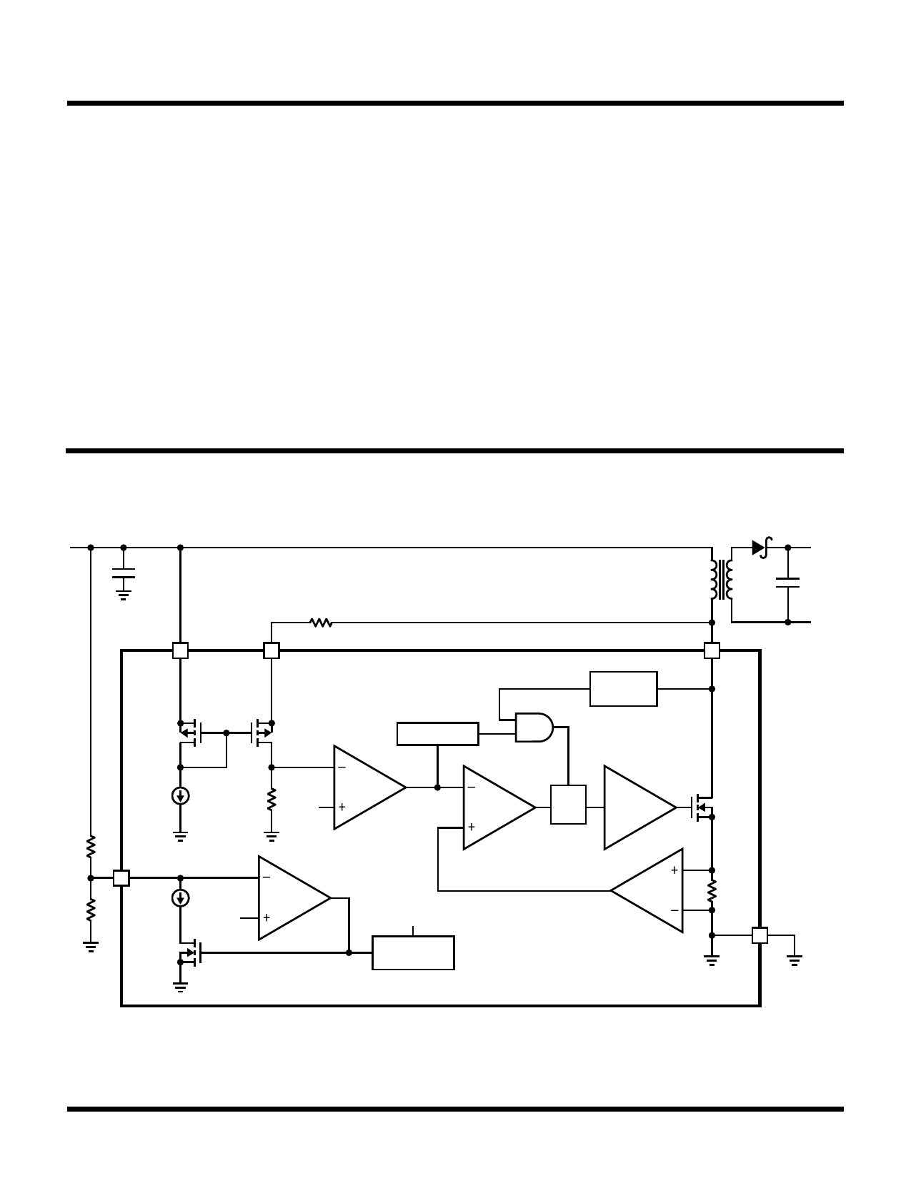
BLOCK DIAGRAM
VIN
CIN
5
VIN
RFB
3
RFB
1:4
M3
M2
25µA
RREF
10kΩ
1.0V
R1
EN/UVLO
1
R2
2.5µA
1.228V
–
A1
+
M4
–
gm
+
OSCILLATOR
–
A3
+
VIN
REFERENCE
REGULATORS
BOUNDARY
DETECTOR
T1
NPS:1
DOUT
LPRI
•
•
LSEC
4
SW
VOUT+
COUT
VOUT–
S
RQ
DRIVER
M1
A2
RSENSE
GND
2
8301 BD
Rev. B
6
For more information www.analog.com
Share Link: 