BR25G128FVM-3GTR 查看數據表(PDF) - ROHM Semiconductor
零件编号
产品描述 (功能)
比赛名单
BR25G128FVM-3GTR Datasheet PDF : 36 Pages
| |||
BR25G128-3
Datasheet
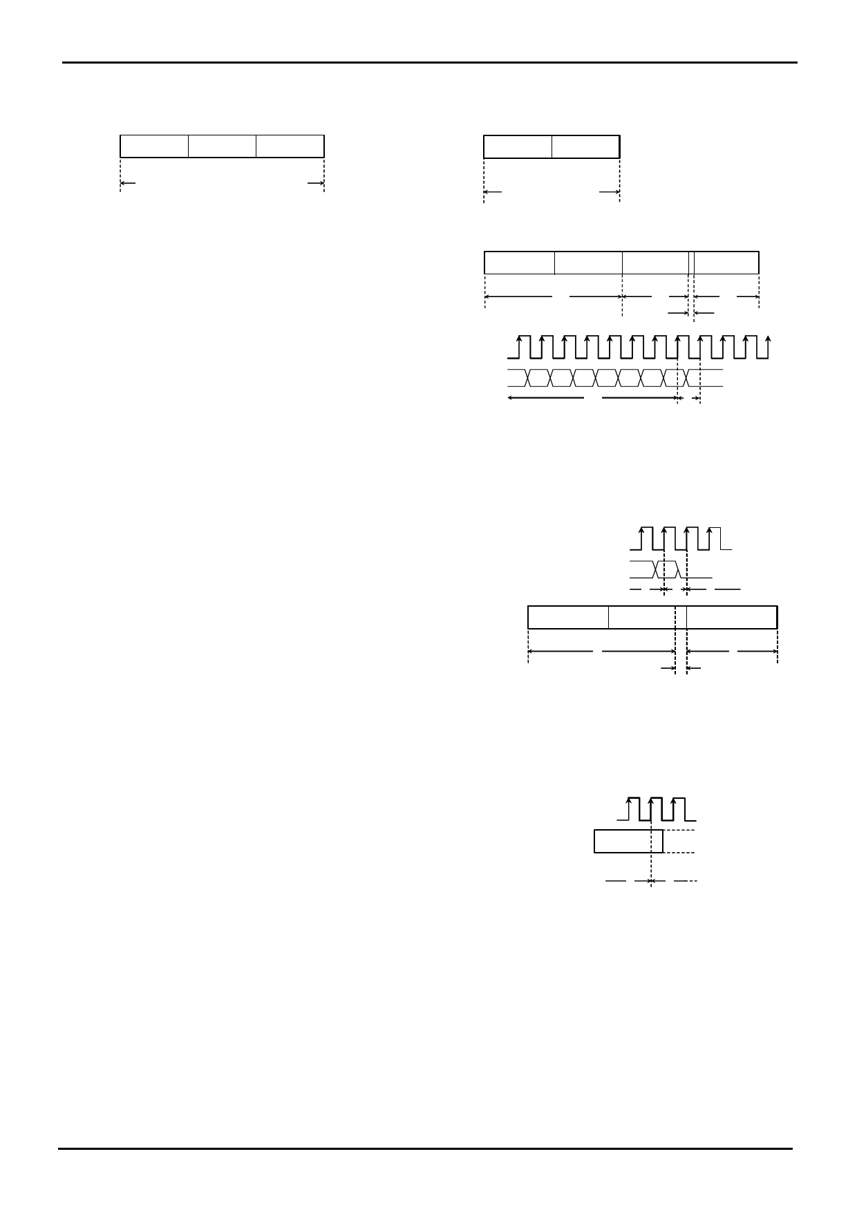
Method to Cancel Each Command
1. READ, RDSR
・Method to cancel : cancel by CSB = “H”.
Ope code
8 bits
Address
16 bits
Data
8 bits
Cancel available in all areas of read mode
Figure 44. READ cancel valid timing
Ope code
Data
8 bits
8 bits
Cancel available in all
areas of rdsr mode
Figure 45. RDSR cancel valid timing
2. WRITE, PAGE WRITE
a:Ope code or address input area
Cancellation is available by CSB=”H”.
b:Data input area (D7 to D1 input area)
Cancellation is available by CSB=”H”.
c:Data input area (D0 area)
In this area, cancellation is not available.
When CSB is set HIGH, write starts.
d:tE/W area
In the area c, by rising CSB, write starts.
While writing, by any input, cancellation cannot be made.
Ope code
8bits
Address
16bits
a
Data
8bits
b
tE/ W
d
c
SCK
SI D7 D6 D5 D4 D3 D2 D1 D0
b
c
Figure 46. WRITE cancel valid timing
Note1) If Vcc is made OFF during write execution, designated address data is not guaranteed, therefore write it once again.
Note2) If CSB is rised at the same timing as that of the SCK rise, write execution / cancel becomes unstable, therefore, it is recommended to rise in
SCK = “L” area. As for SCK rise, assure timing of tCSS / tCSH or more.
3. WRSR
a:From ope code to 15-th clock rise
Cancellation is available by CSB=”H”.
b:From 15-th clock rise to 16-th clock rise (write enable area)
In this area, cancellation is not available by CSB=”H”.
When CSB is set HIGH, write starts using CSB.
c:After 16-th clock rise.
Cancellation is available by CSB=”H”.
However, if write starts (CSB is rised)
In the area b, cancellation cannot be made by any means.
And, by inputting on SCK clock, cancellation cannot be made.
SCK
14 15 16 17
SI
D1 D0
a
b
c
Ope code
Data
tE/W
8 bits
8 bits
a
c
b
Figure 47. WRSR cancel valid timing
Note1) If Vcc is made OFF during write execution, designated address data is not guaranteed, therefore write it once again
Note2) If CSB is rised at the same timing as that of the SCK rise, write execution / cancel becomes unstable, therefore, it is recommended to rise in
SCK = “L” area. As for SCK rise, assure timing of tCSS / tCSH or more.
4. WREN/WRDI
a:From ope code to 7-th clock rise, cancellation is available by CSB = “H”.
b:Cancellation is not available 7-th clock.
SCK
678
Ope code
8 bits
a
b
Figure 48. WREN/WRDI cancel valid timing
www.rohm.com
©2014 ROHM Co., Ltd. All rights reserved.
TSZ22111・15・001
18/32
TSZ02201-0R2R0G100670-1-2
19.Mar.2014 Rev.001
Share Link: 