STW16NB60 查看數據表(PDF) - STMicroelectronics
零件编号
产品描述 (功能)
比赛名单
STW16NB60 Datasheet PDF : 8 Pages
| |||
ELECTRICAL CHARACTERISTICS (CONTINUED)
SWITCHING ON
Symbol
Parameter
td(on)
Turn-on Delay Time
tr
Rise Time
Qg
Total Gate Charge
Qgs
Gate-Source Charge
Qgd
Gate-Drain Charge
Test Conditions
VDD = 300V, ID = 8 A
RG = 4.7Ω, VGS = 10V
(see test circuit, Figure 3)
VDD = 480V, ID = 16 A,
VGS = 10V, RG = 4.7Ω
SWITCHING OFF
Symbol
Parameter
tr(Voff)
Off-voltage Rise Time
tf
Fall Time
tc
Cross-over Time
Test Conditions
VDD = 480V, ID = 16 A,
RG = 4.7Ω, VGS = 10V
(see test circuit, Figure 5)
SOURCE DRAIN DIODE
Symbol
Parameter
Test Conditions
ISD
Source-drain Current
ISDM (2) Source-drain Current (pulsed)
VSD (1) Forward On Voltage
ISD = 16 A, VGS = 0
trr
Qrr
IRRM
Reverse Recovery Time
Reverse Recovery Charge
Reverse Recovery Current
ISD = 16 A, di/dt = 100 A/µs,
VDD = 100V, Tj = 150°C
(see test circuit, Figure 5)
Note: 1. Pulsed: Pulse duration = 300 µs, duty cycle 1.5 %.
2. Pulse width limited by safe operating area.
STW16NB60
Min. Typ. Max. Unit
35
ns
16
ns
80
105
nC
19.5
nC
35
nC
Min.
Typ.
15
12
30
Max.
Unit
ns
ns
ns
Min. Typ. Max. Unit
16
A
64
A
1.6
V
800
ns
11
µC
27
A
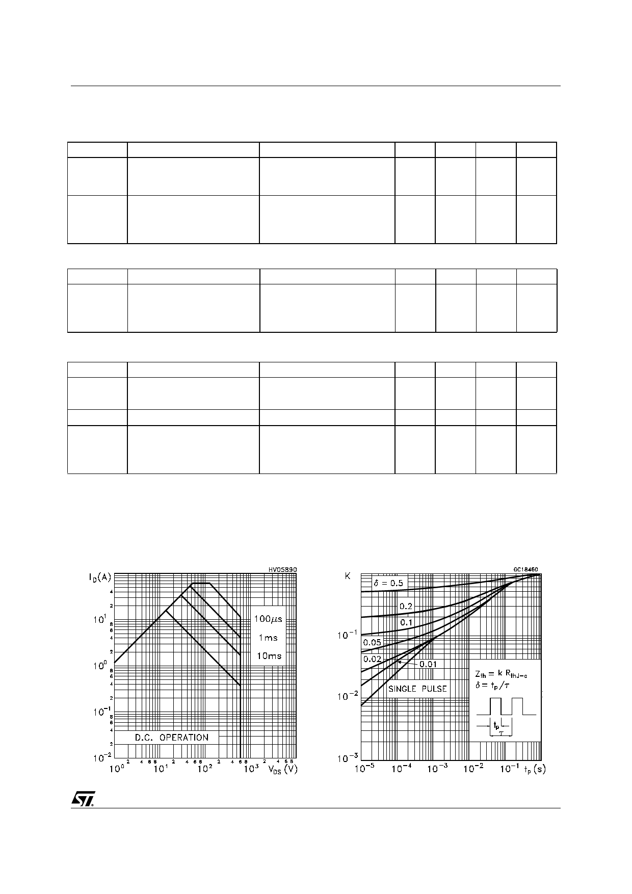
Safe Operating Area
Thermal Impedance
3/8
Share Link: 