STLC1511 查看數據表(PDF) - STMicroelectronics
零件编号
产品描述 (功能)
比赛名单
STLC1511 Datasheet PDF : 31 Pages
| |||
STLC1511
Table 2. Receive Path Specifications
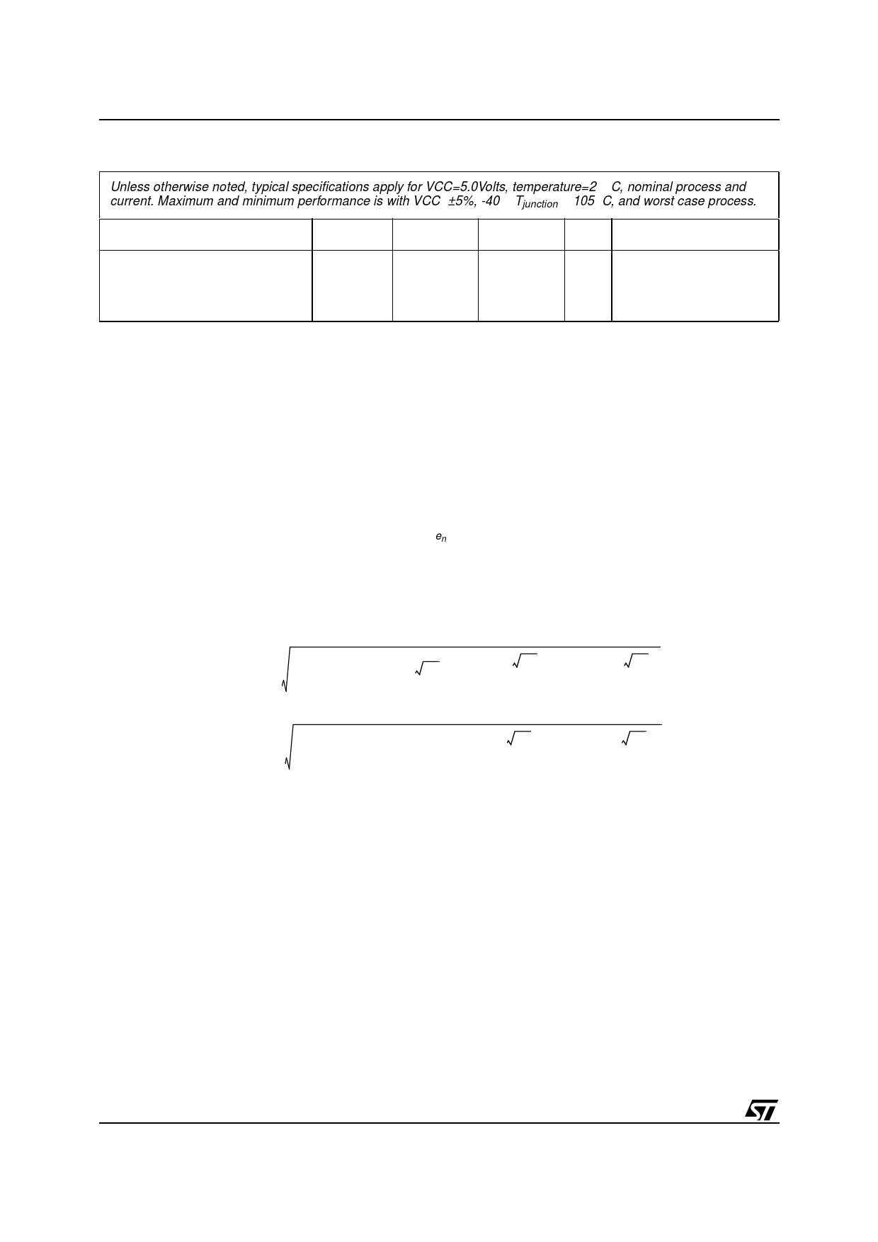
Unless otherwise noted, typical specifications apply for VCC=5.0Volts, temperature=27×C, nominal process and
current. Maximum and minimum performance is with VCC±±5%, -40=<Tjunction=<105×C, and worst case process.
Description
min
typ
max
Units
Comments
Power Up Time18
Rx @ DS19
Rx @ US20
Time to meet output SNR
100
mse requirement
530
c
<1>For the purposes of this specification, a gain of 1 or 0dB is defined as the ratio of the full scale ADC output word to the input voltage
at RXINP/RXINN when the input to the Rx path is at 2.4Vp differential measured between RXINP and RXINN.
<2>For G.lite the STLC1511 will support both CO and CPE applications. As such it needs to support rates from 30kHz to 120kHz (CO
Receive band) and 155kHz to 540kHz (CPE Receive band).
<3>First stage gain is measured from RXINP/RXINN (differential input) to RXOP/RXON (differential output). Note that the gain from
input to output can be adjusted for single ended input or differential input so that the output signal level at the output of the first
stage of the PGA is at full scale. For a single ended input, the unused input, either RXINP or RXINN must be ac coupled to ground.
<4>Second stage gain is measured from RXDCINP/RXDCINN (differential input) to the output of the ADC.
<5>Will be tested at Vcc=5.0V, 27oC, and f=275kHz.
<6>Will be tested at Vcc=5.0V and f=275kHz.
<7>Will be tested at 27oC and f=275kHz.
<8>Will be tested at Vcc=5.0V and 27oC.
<9>Due to 1/f component, the spot noise is maximum at 30kHz over the bands of interest (US and DS).
<10>Noise voltage is specified as the noise spectral density (en) at the input. Conversion to power spectral density is as follows
PSD
=
10
×
log
e1----0n---0-2-
×
1000
<11>Input referred noise assumes that there is a 7dB cut in the first band of aliased noise which falls into the DMT frequencie s and
that higher order aliases are negligible. For example, the single ended input referred noise for the maximum gain setting of 40dB
is calculated as follows:
en =
1
+
-1---0---7-1---⁄--2---0-
( 17 n V
⁄
Hz)2
+
1----7--1--n-0--V--2--0--⁄--⁄--2---H0----z--
2
+
2----5---01---0-n---4-V--0---⁄⁄--2---0--H-----z-
2
In general, the single ended input referred noise can be calculated as follows:
en =
1
+
1----0---7-1---⁄--1---0-
·
( 17 n V
⁄
2
Hz)
+
1----7-1--n-0---V-G----1-⁄---⁄--2-H-0----z--
2
+
1--2--0-5--(--0G---n-1---V-+----G-⁄---2---)H---⁄--2z--0-
2
where G1 and G2 are the gains of the first and second stages of the RxPGA respectively. Note that the assumption of a 7dB cut
on the aliased noise is also used in the above formula and that all other higher order noise is sufficiently suppressed.
<12>Note that the Rx path noise at 0dB gain is dominated by the quantization noise of the ADC and as such there is very little process,
vcc, or temperature dependency and the variation from typical to maximum noise is only due to the Rx PGA.
<13>At maximum gain PGA and Rx input opamp noise are the dominant contributors.
<14>Two tone distortion is measured with two sinewaves with each sinewave at an amplitude of 1/2 full scale. Tone one is at
f1=400kHz and tone two is at f2=500kHz. The two tone distortion requirement is measured from the rms voltage of a single signal
tone to the peak rms voltage of the distortion products.
<15>A multi-tone sine wave is used for the DS Multi-tone test. (The multi-tone signal will be 89 sinewaves equally spaced from
36*4.3125kHz to 125*4.3125kHz with a peak-to-rms ratio of 5.3V/V and an rms voltage equal to 1/5.3 of the peak full scale range
of the PGA.) Multi-tone test measures the difference between the rms voltage of a single tone at the output to the rms voltage of
the peak distortion product at the output in the band of interest.
<16>A multi-tone sine wave is used for the US Multi-tone test. (The multi-tone signal will be 22 sinewaves equally spaced from
7*4.3125kHz to 28*4.3125kHz with a peak-to-rms ratio of 5.3V/V and an rms voltage equal to 1/5.3 of the peak full scale range
of the PGA.) Multi-tone test measures the difference between the rms voltage of a single tone at the output to the rms voltage of
the peak distortion product at the output in the band of interest.
<17>The 1t settling time is roughly equivalent to the unity gain frequency of the PGA block.
<18>The power up time is the time it takes the power up transient to dissipate such that the output SNR specification is met. This time
is dominated by the coupling capacitors at pins RXINP/N and RXDCIP/N.
8/31
Share Link: 