NE8392C 查看數據表(PDF) - Philips Electronics
零件编号
产品描述 (功能)
比赛名单
NE8392C Datasheet PDF : 9 Pages
| |||
Philips Semiconductors
Coaxial transceiver interface for Ethernet/Thin Ethernet
Product specification
NE8392C
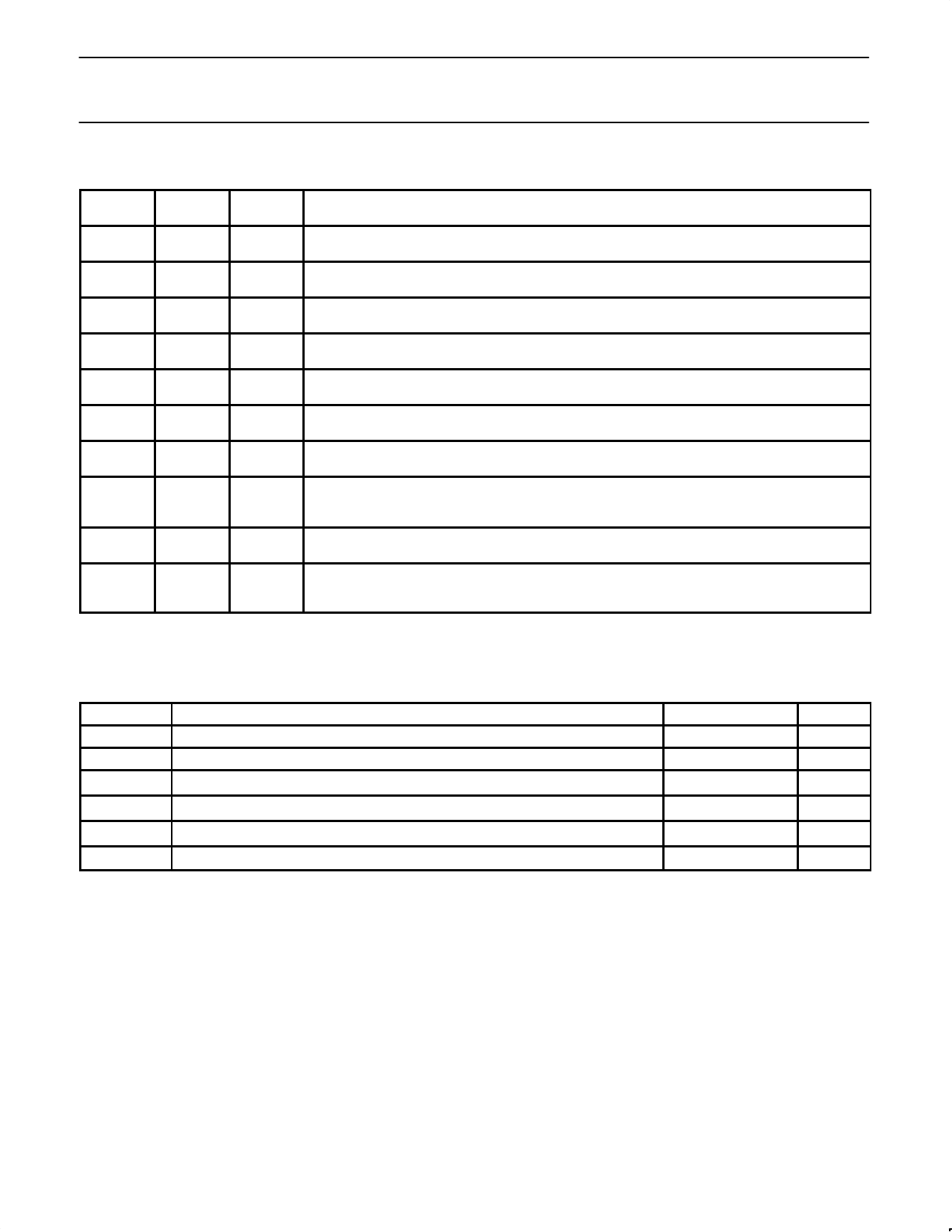
PIN DESCRIPTIONS
PIN NO.
N PKG
PIN NO.
PLCC
SYMBOL
1
2
CD+
2
3
CD–
3
4
RX+
6
12
RX–
7
13
TX+
8
14
TX–
9
15
HBE
11
18
RR+
12
19
RR–
14
26
RXI
15
28
TXO
16
1
CDS
10
16
17
GND
4
5
13
5 to 11
20 to 25
VEE
DESCRIPTION
Collision Outputs. Balanced differential line driver outputs which send a 10MHz oscillation signal to
the DTE in the event of a collision, jabber interrupt or heartbeat test.
Receiver Outputs. Balanced differential line driver outputs which send the received signal to the
DTE.
Transmitter Inputs. Balanced differential line receiver inputs which accept the transmission signal
from the DTE and apply it to the coaxial cable at TXO once it meets Tx squelch threshold.
Heartbeat Enable. The heartbeat function is disabled when this pin is connected to VEE and enabled
when connected to GND or left floating.
External Resistor. A 1kΩ (1%) resistor connected between these pins establishes the signaling
current at TXO. RR– is internally connected to VEE.
Receiver Input. This pin is connected directly to the coaxial cable. Received signals are equalized,
amplified, and sent to the DTE through the RX+ pins once it meets Rx squelch threshold.
Transmitter Output. This pin is connected directly (Thin Ethernet) or through an external isolating
diode (Ethernet) to the coaxial cable.
Collision Detect Sense. Ground sense connection for the collision detection circuitry. This pin
should be directly connected to the coaxial cable shield to prevent ground drops affecting the
collision threshold voltage.
Positive Supply Pin.
Negative supply pins. These pins also serve as a low thermal resistance path for extracting heat
from the die. They should, therefore, be connected to a large metal area on the PC board.
NOTE:
1. The IEEE 802.3 name for CD is CI; for RX is DI; for TX is DO.
ABSOLUTE MAXIMUM RATINGS
SYMBOL
VEE
VIN
Supply voltage1
Voltage at any input1
PARAMETER
TSTG
Storage temperature range
TSOLD
Lead soldering temperature (10sec.)
TJ
Recommended max junction temperature2
θJA
Thermal impedance (N and A packages)
RATING
–12
0 to –12
–65 to +150
+300
+130
60
UNIT
V
V
°C
°C
°C
°C/W
NOTE:
1. 100% measured in production.
2. The junction temperature is calculated from the following expression:
TJ = TA + θJA [VEE (0.08 + n x 0.05/100) + 8(VEE –2) / R]
where
TA =
θJA =
VEE =
n=
Ambient temperature in °C.
Thermal resistance of package.
Normal operating supply voltage in volts.
Percentage transmitter duty cycle.
R = Pull down resistors on the RX and CD pins in Ω.
The N package is specially designed to have a low θJA by directly connecting the four center Pins 4, 5, 12, and 13 to the die attachment area.
These four pins then provide a conductive heat flow path from the die to the PCB where they should be soldered to a large area VEE track. For
the A package, Pins 5 to 11 and 19 to 25 should similarly be soldered to a large area VEE and rack.
1995 May 1
2
Share Link: 