NE8392C 查看數據表(PDF) - Philips Electronics
零件编号
产品描述 (功能)
比赛名单
NE8392C Datasheet PDF : 9 Pages
| |||
Philips Semiconductors
Coaxial transceiver interface for Ethernet/Thin Ethernet
Product specification
NE8392C
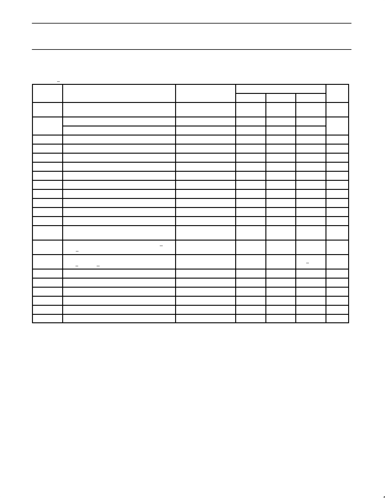
ELECTRICAL CHARACTERISTICS
VEE = –9V +5%; TA = 0°C to +70°C unless otherwise specified1,2. No external isolation
SYMBOL
PARAMETER
LIMITS
TEST CONDITIONS
UNIT
MIN
TYP
MAX
VPOR
IEE
Power–on reset voltage. Transmitter disabled
for |VEE| < |VPOR|
Supply current non–transmitting
Supply current transmitting
–6.5
–80
–125
V
–130
mA
–180
IRXI
ICDS
Receive input bias current
Cable sense input bias current
VRXI = 0V
VCDS = 0V
–2
+25
µA
+2
+6
µA
VIH
HBE input HIGH voltage
VEE +1.4
V
VIL
IIH
IIL
ITDC
ITAC
ITX10
VTCOM
VCD
HBE input LOW voltage
HBE input HIGH current
HBE input LOW current
Transmit output DC current level3
Transmit output AC current level3
Transmit current
Transmitter output voltage compliance4
Collision threshold5
VHBE = 0V
VHBE = VEE
VTXO = –10V
–37
±28
–250
Measured by applying
DC voltage at RXI
–1450
250
–500
–41
VEE +0.4
V
500
µA
–1000
µA
–45
mA
±ITDC
mA
+250
µA
–3.7
V
–1530
–1580
mV
VOD
Differential output voltage – non idle at RX+ and
CD+6
±600
±1200
mV
VOB
Differential output voltage imbalance – idle at
RX+ and CD+7
+40
mV
VOC
VRS
VTS
RRXI
CRXI
RTXO
Output common mode voltage at RX± and CD±
Receiver squelch threshold
Transmitter squelch threshold
Shunt resistance at RXI non–transmitting
Input capacitance at RXI
Shunt resistance at TXO transmitting
VRXI average DC
(VTX+ – VTX–) peak
–1.5
–130
–175
100
–2
–250
–225
2
10
–2.5
V
–370
mV
–300
mV
kΩ
pF
kΩ
NOTES:
1. Currents flowing into device pins are positive. All voltages are referenced to ground unless otherwise specified. For ease of interpretation,
the parameter limit that appears in the MAX column is the largest value of the parameter, irrespective of sign. Similarly, the value in the MIN
column is the smallest value of the parameter, irrespective of sign.
2. All typicals are for VEE = –9V and TA = 27°C.
3. ITDC is measured as (VMAX + VMIN)/(2 x 25) where VMAX and VMIN are the max and min voltages at TXO with a 25Ω load between TXO and
GND. ITAC is measured as (VMAX – VMIN)/(2 x 25).
4. The TXO pin shall continue to sink at least ITDC min when the idle (no signal) voltage on this pin is –3.7V.
5. Collision threshold for an AC signal is within 10% of VCD.
6. Measured on secondary side of isolation transformer (see Connection Diagram, Figure 1). The transformer has a 1:1 turns ratio with an
inductance between 30 and 100µH at 5MHz.
7. Measured as the voltage difference between the RX pins or the CD pins with the transformer removed.
1995 May 1
4
Share Link: 