NE8392C 查看數據表(PDF) - Philips Electronics
零件编号
产品描述 (功能)
比赛名单
NE8392C Datasheet PDF : 9 Pages
| |||
Philips Semiconductors
Coaxial transceiver interface for Ethernet/Thin Ethernet
Product specification
NE8392C
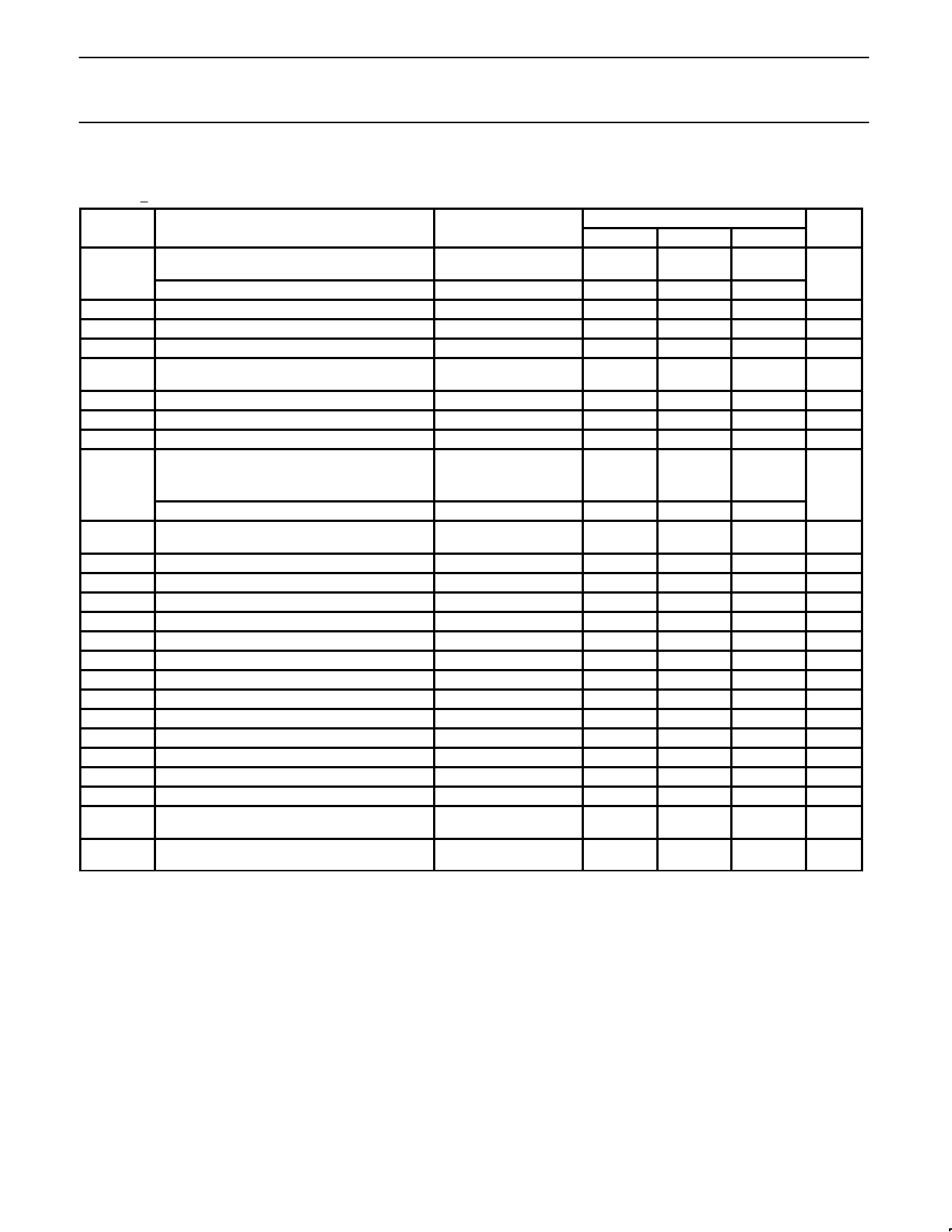
TIMING CHARACTERISTICS
VEE = –9V +5%; TA = 0 to 70°C, unless otherwise specified1. No external isolation diode on TXO.
SYMBOL
PARAMETER
TEST CONDITIONS
MIN
tRON
Receiver start up delay RXI to RX± (Figure 3)
First received bit on RX±
First validly timed bit on RX±
VRXI = –2V peak
tRD
Receiver prop. delay RXI to RX±
VRXI = –2V peak
tRR
Differential output rise time on RX± and CD±2,3
tRF
Differential output fall time on RX± and CD±2,3
tOS
Differential output settling time on RX± and CD±
to VOB = 40mV2 (see Figure 4)
tRJ
Receiver and cable total jitter
tRHI
Receiver high to idle time
Measured to +210mV
150
tRM
Rise and fall time matching on RX± and CD±
tRF – tRR
Transmitter start–up delay TX± to TXO
(Figure 5)
tTST
First transmitted bit on TXO
VTX± = –1V peak
First validly timed bit
tTD
Transmitter prop delay TX± to TXO
(see Figure 5)
VTX± = 1V peak
tTR
Transmitter rise time 10% to 90% (see Figure 5)
tTF
Transmitter fall time 10% to 90% (see Figure 5)
tTM
tTF – tTR mismatch
tTS
Transmitter added skew4
tTON
Transmitter turn on pulse width (see Figure 5)
VTX± = 1V peak
10
tTOFF
Transmitter turn off pulse width (see Figure 5)
VTX± = 1V peak
150
tCON
Collision turn on delay (see Figure 6)
0V to –2V step at RXI
tCOFF
Collision turn off delay (see Figure 6)
–2V to 0V step at RXI
tCHI
Collision high to idle time (see Figure 6)
Measured to +210mV
150
fCD
Collision frequency (see Figure 6)
8.0
tCP
Collision signal pulse width (see Figure 6)
35
tHON
Heartbeat turn on delay (see Figure 7)
0.6
tHW
Heartbeat test duration (see Figure 7)
0.5
tJA
Jabber activation delay measured from TX± to
CD± (see Figure 8)
20
tJR
Jabber reset delay measured from TX± to CD±
(see Figure 8)
250
LIMITS
TYP
35
5
5
1
±3
0.4
MAX
5
tRON +2
50
850
UNIT
bits
ns
ns
ns
µs
ns
ns
ns
1
2
bits
tTST + 2
35
50
ns
25
ns
25
ns
±2
ns
±2
ns
40
ns
250
340
ns
13
bits
16
bits
850
ns
10
12.5
MHz
70
ns
1.6
µs
1.5
µs
60
ms
750
ms
NOTES:
1. All typicals are for VEE = –9V and TA = 27°C.
2. Measured on secondary side of isolation transformer (see Figure 1, Connection Diagram). The transformer has a 1:1 turn ratio with an
inductance between 30 and 100µH at 5MHz.
3. The rise and fall times are measured as the time required for the differential voltage to change from –225mV to +225mV, or +225mV to
–225mV, respectively.
4. Difference in propagation delay between rising and falling edges at TXO.
FUNCTIONAL DESCRIPTION
The NE8392C contains four main functional blocks (see Block
Diagram). These are:
a. The receiver which takes data from the coaxial cable and sends
it to the DTE.
b. The transmitter which receives data from the DTE and sends it
onto the coaxial cable.
c. The collision detection and heartbeat generation circuitry which
indicates to the DTE any collision on the coaxial cable and tests
for collision circuitry functionality at the end of every
transmission.
d. The jabber timer which disables the transmitter in the event of a
longer than legal length data packet.
Receiver Functions
The receiver consists of an input buffer, a cable equalizer, a 4-pole
Bessel low pass filter, a squelch circuit and a differential line driver.
The buffer provides high input resistance and low input capacitance
to minimize loading and reflections on the coaxial cable.
1995 May 1
5
Share Link: 