HS-80C86RH(1995) 查看數據表(PDF) - Intersil
零件编号
产品描述 (功能)
比赛名单
HS-80C86RH Datasheet PDF : 37 Pages
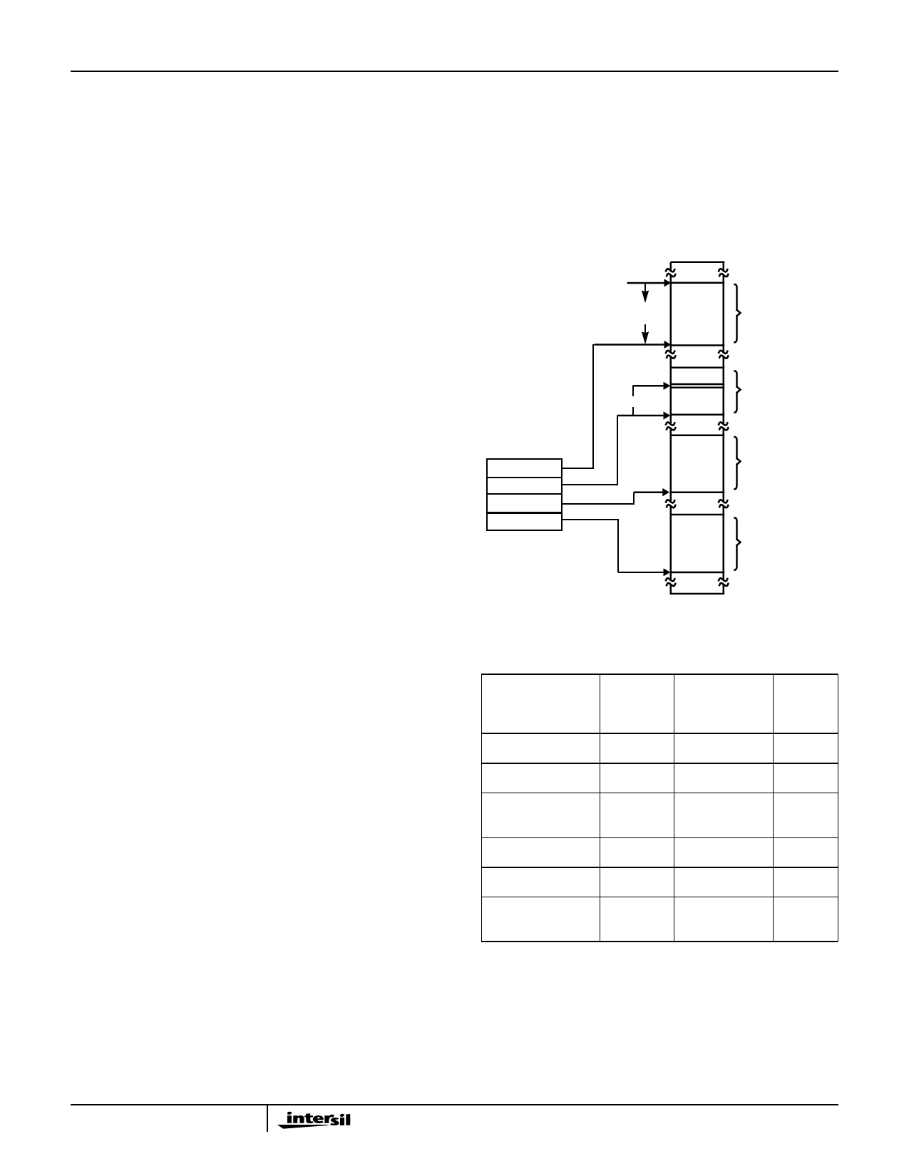
| |||
HS-80C86RH
External Interface
Processor RESET and lnitialization
Processor initialization or start up is accomplished with acti-
vation (HIGH) of the RESET pin. The HS-80C86RH RESET
is required to be HIGH for greater than 4 CLK cycles. The
HS-80C86RH will terminate operations on the high-going
edge of RESET and will remain dormant as long as RESET
is HIGH. The low-going transition of RESET triggers an
internal reset sequence for approximately 7 CLK cycles.
After this interval, the HS-80C86RH operates normally
beginning with the instruction in absolute location FFFFOH.
(See Figure 2). The RESET input is internally synchronized
to the processor clock. At initialization, the HIGH-to-LOW
transition of RESET must occur no sooner than 50µs (or
4 CLK cycles, whichever is greater) after power-up, to allow
complete initialization of the HS-80C86RH.
NMl will not be recognized prior to the second clock cycle fol-
lowing the end of RESET. If NMI is asserted sooner than
9 CLK cycles after the end of RESET, the processor may
execute one instruction before responding to the interrupt.
Bus Hold Circuitry
To avoid high current conditions caused by floating inputs to
CMOS devices and to eliminate need for pull- up/down resis-
tors, “bus-hold” circuitry has been used on the HS-80C86RH
pins 2-16, 26-32 and 34-39. (See Figure 4A and 4B). These
circuits will maintain the last valid logic state if no driving
source is present (i.e. an unconnected pin or a driving
source which goes to a high impedance state). To overdrive
the “bus hold” circuits, an external driver must be capable of
supplying approximately 400µA minimum sink or source cur-
rent at valid input voltage levels. Since this “bus hold” cir-
cuitry is active and not a “resistive” type element, the
associated power supply current is negligible and power dis-
sipation is significantly reduced when compared to the use
of passive pull-up resistors.
OUTPUT
DRIVER
BOND
PAD
EXTERNAL
PIN
INPUT
BUFFER
INPUT
PROTECTION
CIRCUITRY
FIGURE 4A. BUS HOLD CIRCUITRY PIN 2-16, 34-39
VCC P
OUTPUT
DRIVER
BOND
PAD
EXTERNAL
PIN
INPUT
BUFFER
INPUT
PROTECTION
CIRCUITRY
FIGURE 4B. BUS HOLD CIRCUITRY PIN 26-32
Interrupt Operations
Interrupt operations fall into two classes: software or hard-
ware initiated. The software initiated interrupts and software
aspects of hardware interrupts are specified in the Instruc-
tion Set Description. Hardware interrupts can be classified
as non-maskable or maskable.
Interrupts result in a transfer of control to a new program
location. A 256-element table containing address pointers to
the interrupt service routine locations resides in absolute
locations 0 through 3FFH, which are reserved for this pur-
pose. Each element in the table is 4 bytes in size and corre-
sponds to an interrupt “type”. An interrupting device supplies
an 8-bit type number during the interrupt acknowledge
sequence, which is used to “vector” through the appropriate
element to the interrupt service routine location. All flags and
both the Code Segment and Instruction Pointer register are
saved as part of the INTA sequence. These are restored
upon execution of an Interrupt Return (lRET) instruction.
Non-Maskable Interrupt (NMI)
The processor provides a single non-maskable interrupt pin
(NMl) which has higher priority than the maskable interrupt
request pin (INTR). A typical use would be to activate a
power failure routine. The NMl is edge-triggered on a LOW-
to-HIGH transition. The activation of this pin causes a type 2
interrupt.
NMl is required to have a duration in the HIGH state of
greater than 2 CLK cycles, but is not required to be synchro-
nized to the clock. Any positive transition of NMl is latched
on-chip and will be serviced at the end of the current instruc-
tion or between whole moves of a block-type instruction.
Worst case response to NMl would be for multiply, divide,
and variable shift instructions. There is no specification on
the occurrence of the low-going edge; it may occur before,
during or after the servicing of NMl. Another positive edge
triggers another response if it occurs after the start of the
NMl procedure. The signal must be free of logical spikes in
general and be free of bounces on the low-going edge to
avoid triggering extraneous responses.
Maskable Interrupt (INTR)
The HS-80C86RH provides a single interrupt request input
(INTR) which can be masked internally by software with the
resetting of the interrupt enable flag (IF) status bit. The inter-
rupt request signal is level triggered. It is internally synchro-
nized during each clock cycle on the high-going edge of
CLK. To be responded to, INTR must be present (HIGH) dur-
ing the clock period preceding the end of the current instruc-
tion or the end of a whole move for a block- type instruction.
INTR may be removed anytime after the falling edge of the
first INTA signal. During the interrupt response sequence fur-
ther interrupts are disabled. The enable bit is reset as part of
the response to any interrupt (INTR, NMl, software interrupt
or single-step), although the FLAGS register which is auto-
matically pushed onto the stack reflects the state of the pro-
cessor prior to the interrupt. Until the old FLAGS register is
restored the enable bit will be zero unless specifically set by
an instruction.
Spec Number 518055
871
Share Link: 