BIT3713 查看數據表(PDF) - Unspecified
零件编号
产品描述 (功能)
比赛名单
BIT3713 Datasheet PDF : 11 Pages
| |||
Beyond Innovation Technology Co., Ltd.
Note 1. The output driver frequency is the half of the ramp wave frequency.
Note 2. Only verified by simulation. Not 100% tested.
Note 3. The voltages of the output drivers are pulled to GND in each off states.
BIT3713
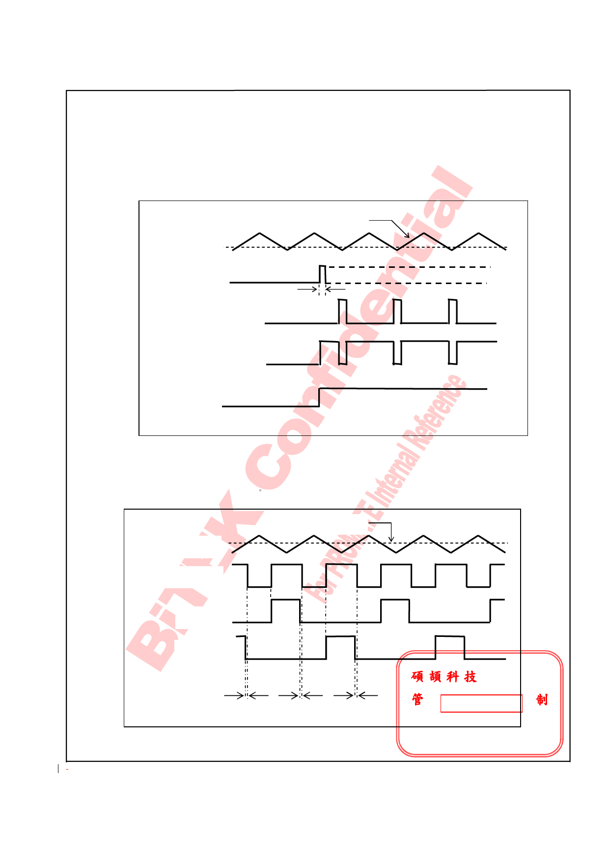
Timing Diagram
The timing of the 2nd low frequency PWM generator, ISEN and LOAD pin are as bellow: A 51Kohm
pulled-low resistor is connected on PWMOUT pin in this example.
CTPWM
PWMDC
ISEN
<1.3V
>1.3V
PWMOUT(MODE=0)
>0.1 us
PWMOUT(MODE=1)
(SW close)
(SW open)
Fig. 3
BIT3713 uses fixed frequency driving methodology. The power switch is driven by fixed frequency PWM
controlled signal. The detail timing relationship is shown as bellow: The maximum duty cycle of OUT1 and
OUT1 are smaller than 50% with 180 phase difference.
Ramp Wave
CMP_PWM Output
Err_Amp Output
‘05/12/15
Preliminary
OUT1
OUT2
delay
delay
delay
Fig. 4
Confidential, for authorized user only
BiTEK
December 20, 2005
DCC CONTROLLED
page 8 of 11
Share Link: 