FS6261-01 查看數據表(PDF) - AMI Semiconductor
零件编号
产品描述 (功能)
比赛名单
FS6261-01 Datasheet PDF : 17 Pages
| |||
X T
)6
0RWKHUERDUG &ORFN *HQHUDWRU ,&
January 2000
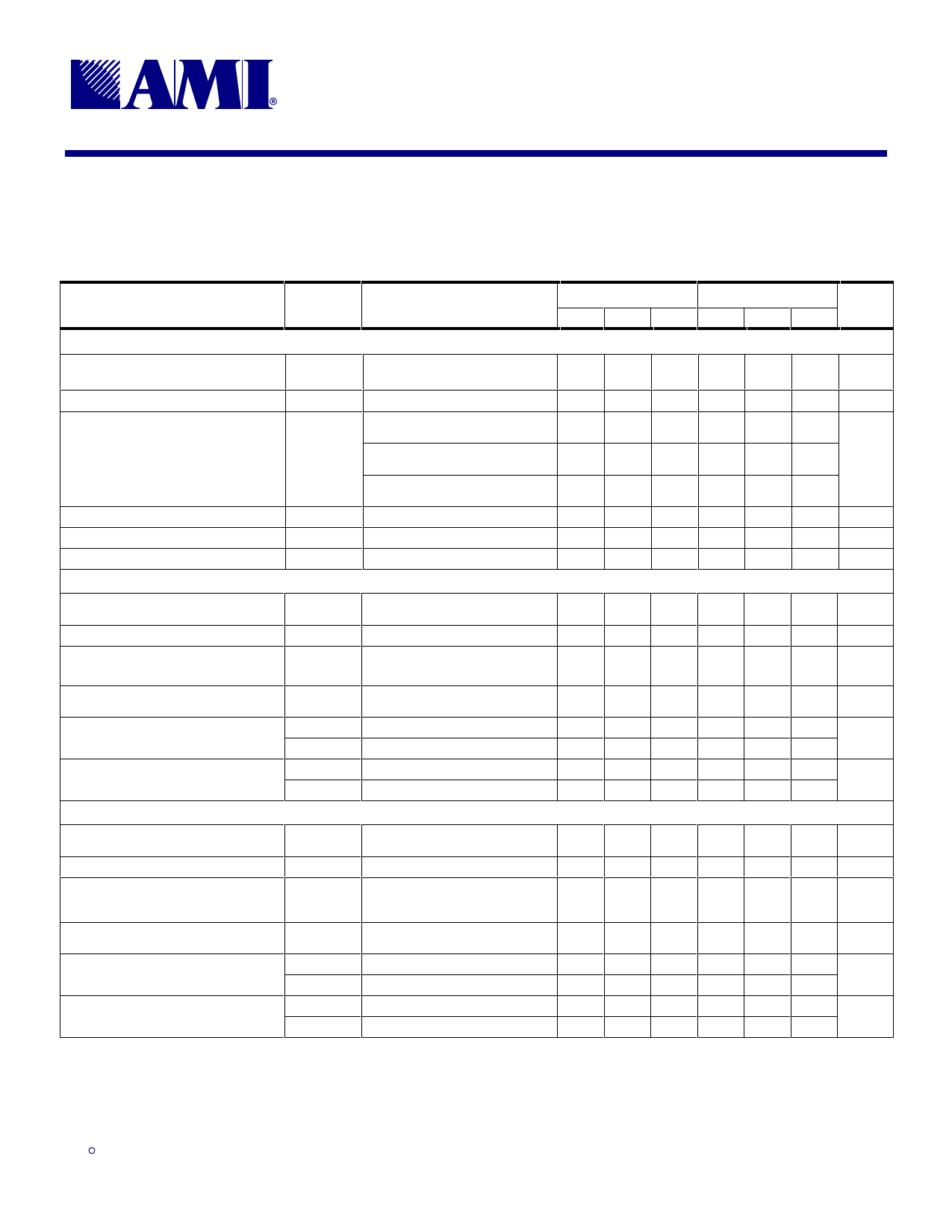
Table 9: AC Timing Specifications
Unless otherwise stated, all power supplies = 3.3V ± 10%, no load on any output, and ambient temperature range TA = 0°C to 70°C. Parameters denoted with an asterisk ( * ) represent nominal
characterization data and are not currently production tested to any specific limits. MIN and MAX characterization data are ± 3σ from typical. Negative currents indicate current flows out of the device.
Spread spectrum modulation is disabled except for Rise/Fall time measurements.
PARAMETER
SYMBOL
CONDITIONS/DESCRIPTION
133MHz
MIN. TYP. MAX.
100MHz
MIN. TYP. MAX.
UNITS
Overall
Spread Spectrum Modulation
Frequency *
fm
SS_EN# low
31.5
31.5 kHz
Spread Spectrum Modulation Index*
δm
SS_EN# low
-0.5
-0.5
%
CPU @ 1.25V, CL=20pF to CK66 @
1.5V, CL=30pF (rising edges)
0
0.3 1.5
0
0.4 1.5
Clock Offset
tpd
CK66 @ 1.5V, CL=30pF to PCI @
1.5V, CL=30pF (rising edges)
1.5 2.9 4.0 1.5 3.1 4.0
ns
CPU @ 1.25V, CL=20pF to APIC @
1.25V, CL=20pF (rising edges)
1.5
2.3
4.0
1.5
3.3
4.0
Tristate Enable Delay *
tDZL, tDZH SEL_0:1 and SEL_133/100#=0
1.0
10 1.0
10
ns
Tristate Disable Delay *
tDZL, tDZH SEL_0:1 and SEL_133/100#=0
1.0
10 1.0
10
ns
Clock Stabilization (on power-up) *
tSTB
via PWR_DWN#
3.0
3.0
ms
APIC_0:2 Clock Output (2.5V Type 1 Clock Buffer)
Duty Cycle *
dt
Ratio of high pulse width to one
clock period, measured at 1.5V
45
50
55
45
50
55
%
Clock Skew *
Jitter, Long Term (σy(τ)) *
Jitter, Period (peak-peak) *
Rise Time *
Fall Time *
tskw
tj(LT)
tj(∆P)
tr min
tr max
tf min
tf max
APIC to APIC @ 1.25V, CL=20pF
On rising edges 500µs apart at 1.25V
relative to an ideal clock, CL=20pF, all
PLLs active
From rising edge to rising edge at
1.25V, CL=20pF, all PLLs active
Measured @ 0.4V – 2.0V; CL=10pF
Measured @ 0.4V – 2.0V; CL=20pF
Measured @ 2.0V – 0.4V; CL=10pF
Measured @ 2.0V – 0.4V; CL=20pF
-70
204
82
1.2
1.5
1.8
2.1
-70
122
ps
88
ps
1.2
ns
1.5
1.5
ns
1.8
CPU/2_0:1 Clock Outputs (2.5V Type 1 Clock Buffer)
Duty Cycle *
Clock Skew *
Jitter, Long Term (σy(τ)) *
Jitter, Period (peak-peak) *
Rise Time *
Fall Time *
dt
Ratio of high pulse width to one
clock period, measured at 1.5V
45
52
55
45
52
55
%
tskw
CPU/2 to CPU/2 @ 1.25V, CL=20pF
+10
+10
On rising edges 500µs apart at
tj(LT)
1.25V relative to an ideal clock,
136
CL=20pF, all PLLs active
122
ps
tj(∆P)
From rising edge to rising edge at
1.25V, CL=20pF, all PLLs active
108
112
ps
tr min
Measured @ 0.4V – 2.0V; CL=10pF
0.9
tr max
Measured @ 0.4V – 2.0V; CL=20pF
1.1
0.8
ns
1.1
tf min
Measured @ 2.0V – 0.4V; CL=10pF
1.0
tf max
Measured @ 2.0V – 0.4V; CL=20pF
1.2
1.0
ns
1.2
,62
11
1.31.00
Share Link: 