5962F9563501QYC 查看數據表(PDF) - Intersil
零件编号
产品描述 (功能)
比赛名单
5962F9563501QYC Datasheet PDF : 36 Pages
| |||
HS-RTX2010RH
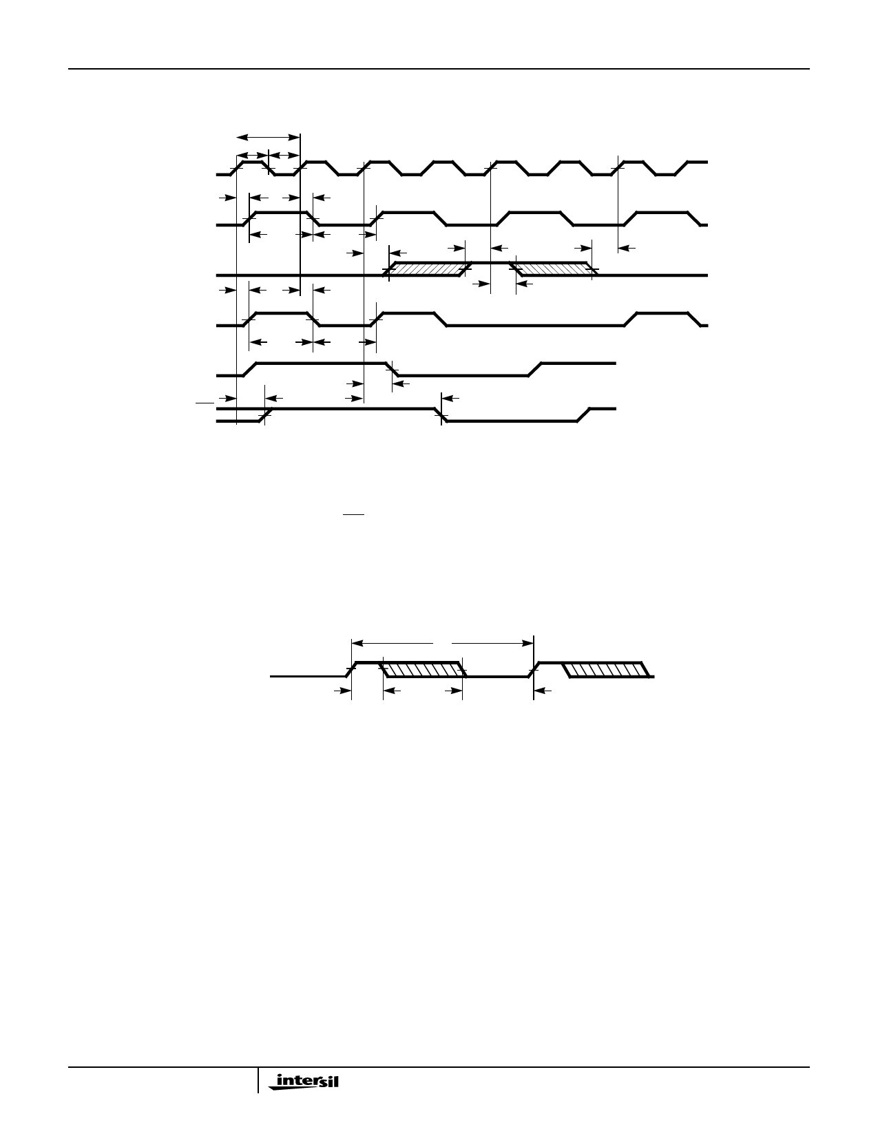
Timing Diagrams
ICLK
t1
t2
t3
t11
t19
TCLK
t13
t12
t5
t4
t4
WAIT
t15
t20
t5
PCLK
(NOTE 1)
PCLK
(NOTE 2)
GIO
(NOTE 3)
t17
t16
t51
t20
t50
NOTES:
1. NORMAL CYCLE: This waveform describes a normal PCLK cycle and a PCLK cycle with a Wait state.
2. EXTENDED CYCLE: This waveform describes a PCLK cycle for a USER memory access or an external ASIC Bus read cycle when the CYCEXT
bit or ARCE bit is set.
3. EXTENDED CYCLE: This waveform describes a GIO cycle for an external ASIC Bus read when the ARCE bit is set.
4. An active HIGH signal on the RESET input is guaranteed to reset the processor if its duration is greater than or equal to 4 rising edges of ICLK
plus 1/2 ICLK cycle setup and hold times. If the RESET input is active for less than four rising edges of ICLK, the processor will not reset.
FIGURE 2. CLOCK AND WAIT TIMING
EI5 - EI3
t6
t7
t8
FIGURE 3. TIMER/COUNTER TIMING
6
Share Link: 