GS82032 查看數據表(PDF) - Giga Semiconductor
零件编号
产品描述 (功能)
比赛名单
GS82032 Datasheet PDF : 23 Pages
| |||
GS82032AT/Q-180/166/133/100
AC Test Conditions
Parameter
Conditions
Input high level
2.3 V
Input low level
0.2 V
Input slew rate
1 V/ns
Input reference level
1.25 V
Output reference level
1.25 V
Output load
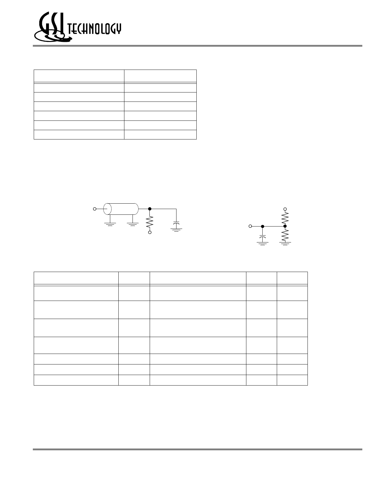
Fig. 1& 2
Notes:
1. Include scope and jig capacitance.
2. Test conditions as specified with output loading as shown in Fig. 1 unless otherwise noted.
3. Output Load 2 for tLZ, tHZ, tOLZ and tOHZ
4. Device is deselected as defined by the Truth Table.
Output Load 1
DQ
Output Load 2
2.5 V
50Ω
30pF*
DQ
225Ω
VT = 1.25 V
* Distributed Test Jig Capacitance
5pF* 225Ω
DC Electrical Characteristics
Parameter
Input Leakage Current
(except mode pins)
ZZ Input Current
Symbol
IIL
IINZZ
Mode Pin Input Current
IINM
Output Leakage Current
IOL
Output High Voltage
VOH
Output High Voltage
VOH
Output Low Voltage
VOL
Test Conditions
VIN = 0 to VDD
VDD ≥ VIN ≥ VIH
0V ≤ VIN ≤ VIH
VDD ≥ VIN ≥ VIL
0V ≤ VIN ≤ VIL
Output Disable,
VOUT = 0 to VDD
IOH = –4 mA, VDDQ = 2.375 V
IOH = –4 mA, VDDQ = 3.135 V
IOL = 4 mA
Min
–1 uA
–1 uA
–1 uA
–300 uA
–1 uA
–1 uA
1.7 V
2.4 V
Max
1 uA
1 uA
300 uA
1 uA
1 uA
1 uA
0.4 V
Rev: 1.09 7/2002
11/23
© 2000, Giga Semiconductor, Inc.
Specifications cited are subject to change without notice. For latest documentation see http://www.gsitechnology.com.
Share Link: 