AD6426 查看數據表(PDF) - Analog Devices
零件编号
产品描述 (功能)
比赛名单
AD6426 Datasheet PDF : 50 Pages
| |||
Preliminary Technical Information
GENERAL CONTROL
Clocks
Clock Input
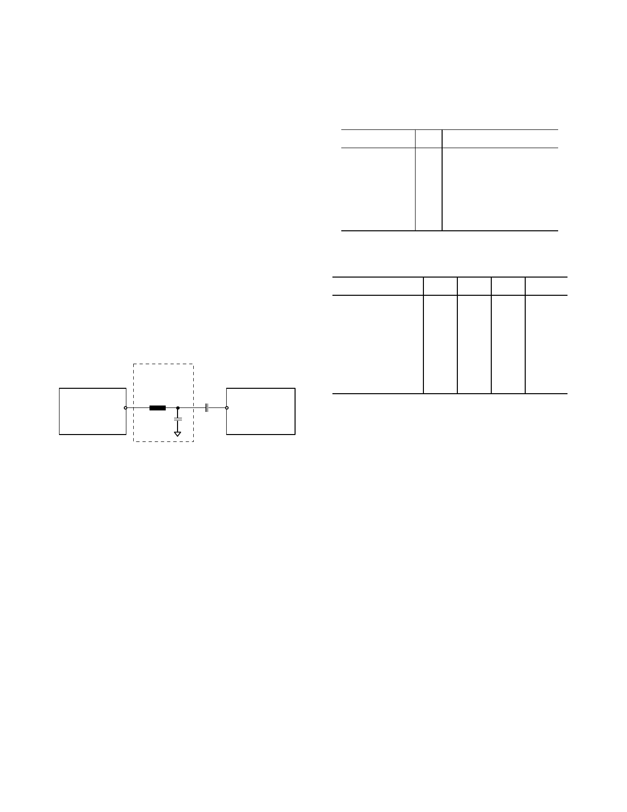
The AD6426 requires a single 13 MHz, low level clock signal,
which has to be provided at the pin CLKIN. For proper
operation a signal level of 250 mVPP minimum is required.
This feature eases system design and reduces the need for
external clock buffering. Only minimal external components
are required as shown in Figure 4.
The internal clock buffer can accept any regular waveform as
long as it can find voltage points in the signal, for which a
50% duty cycle can be determined. This condition is met for
sinewaves, triangles, or slew-limited square waves. Dedicated
circuitry searches for these points and generates the respective
bias voltage internally.
The external capacitor (1nF) decouples the bias voltage of the
clock signal generated by the oscillator from the internally
generated bias voltage of the clock buffer circuitry.
The LC-filter shown is optional. It ensures, that the input
signal is “well behaved” and sinusoidal. Additionally it filters
out harmonics and noise, that may be on top of the pure 13
MHz signal.
Optional
13 MHz Filter
13 MHz OUT
VCTCXO
2.2 µH
68 pF
1nF
CLKIN AD6422
Figure 4. Clock Input Circuitry
Clock Output
The input clock drives both the H8 and the Channel Codec
directly. A gated version, controlled by the Output Clock
Enable flag in CC Control Register 45, drives the CLKOUT
pin of the EVBC interface. The stand-by state of CLKOUT is
logic zero. The CLKOUT output will be active on reset.
Slow Clocking
To reduce power consumption of AD20msp425 solutions, a
new slow clocking scheme has been designed into the
AD6426. This scheme allows the VCTCXO to be powered
down between paging blocks during Idle Mode and for a
32.768kHz oscillator to keep the time reference during this
period. Only a common 32.768kHz watch crystal is required to
take advantage of this scheme. As in previous generations,
power consumption is also kept to a minimum using
asynchronous design techniques and by stopping all
unnecessary clocks.
Layer 1 software and logic built into the AD6426 are
responsible for maintaining synchronization and calibration of
the slow clock and ensure the validity of the time reference
AD6426
under all circumstances. The active-high OSC13MON output
is prevented from becoming inactive if the 32.768kHz signal is
not present. The following table describes the functionality of
the relevant pins.
Name
OSCIN
OSCOUT
OSC13MON
PWRON
I/O Function
I 32.768kHz Crystal Input
O 32.768kHz Oscillator
Output
O 13 MHz Oscillator Power
Control
O Power ON/OFF Control
The following table lists the recommended specification for a
32kHz crystal.
Parameter
ESR
Shunt Capacitance
Load Capacitance
Turnover
Temperature (To)
Parabolic Curvature
Constant (K)
Min Typ Max Units
50
kΩ
2
pF
6 12.5 30
pF
25
°C
0.040
ppm/°C
Real Time Clock and Alarm
The AD6426 provides a simple Real Time Clock (RTC) using
the 32.768kHz clock input. A 40 bit counter allows for more
than one year of resolution. The RTC module contains a
32.768kHz on chip oscillator buffer designed for very low
power consumption and a set of registers for a timer, alarm,
control and status functions.
The RTC circuit is supplied by two sources; a VDDRTC
supply pin and the main system VDD. It is the handset
designer’s responsibility to provide suitable switching
between the main system VDD and a backup supply to ensure
the RTC module is permanently powered.
The VDDRTC pin is intended to interface to a backup battery
circuit or charge holding network in order for the RTC to
maintain timing accuracy when the main battery is removed
and the handset is powered down.
The user can set an alarm time at which the handset powers
up. If an alarm time is set, the current time matches the alarm
time, and the power on alarm feature is enabled, the handset is
powered up by asserting the PWRON pin for a period of
approximately 2 seconds.
This Information applies to a product under development. Its characteristics and specifications are subject to change without notice. Analog Devices assumes no
obligation regarding future manufacture unless otherwise agreed to in writing. No responsibility is assumed by Analog Devices for its use; nor for any
infringements of patents or other rights of third parties which may result from its use. No license is granted by implication or otherwise under any patent or patent
rights of Analog Devices.
Revision Preliminary 2.3 (June 9, ´98)
- 14 -
Confidential Information
Share Link: 