AD8158 查看數據表(PDF) - Analog Devices
零件编号
产品描述 (功能)
比赛名单
AD8158 Datasheet PDF : 36 Pages
| |||
AD8158
Table 7. Register Address 0x0F
Bit 7
Bit 6
Bit 5
Set to 0
Set to 0
Set to 0
Bit 4
Set to 0
Bit 3
Set to 0
Bit 2
Set to 0
Bit 1
MODE[1]
Bit 0
MODE[0]
Function
Mode
Table 8. Setting the Control Interface Mode
Mode 1
Mode 0
Control Mode
0
0
Pin control
0
1
Mixed control
1
1
Serial control
THE SWITCH
(MUX/DEMUX/UNICAST/BICAST/LOOPBACK)
The mux and demux functions of the AD8158 can be controlled
either with the toggle pins or through the register map. The
multiplexer path switches received data from Input Port A or
Input Port B to Output Port C. The SEL[3:0] pins allow switching
lanes independently. The demultiplexer path switches received
data from Input Port C to Output Port A, Output Port B, or (if
bicast mode is enabled) to both Output Port A and Output Port B.
Table 9. Port Selection and Configuration with All
Loopbacks Disabled
BICAST
Output
SELx Port A
Output
Port B
Output
Port C
0
0
Ix_C[3:0] Idle
Ix_A[3:0]
0
1
Idle
Ix_C[3:0] Ix_B[3:0]
1
0
Ix_C[3:0] Ix_C[3:0] Ix_A[3:0]
1
1
Ix_C[3:0] Ix_C[3:0] Ix_B[3:0]
When the device is in unicast mode, the output lanes on either
Port A or Port B are in an idle state. In the idle state, the output
tail current is set to 0, and the P and N sides of the lane are
pulled up to the output termination voltage through the on-chip
termination resistors. To save power, the unused receiver
automatically disables.
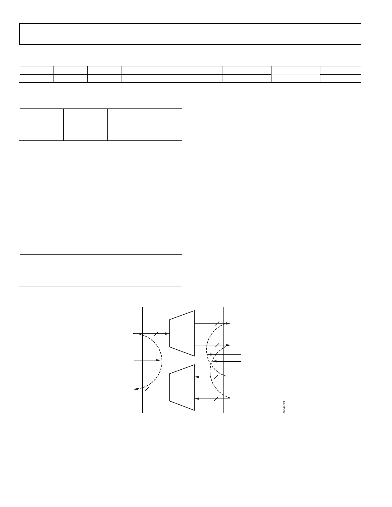
The AD8158 supports port-level loopback, illustrated in Figure 36.
The loopback control pins override the lane select (SEL[3:0])
and bicast control (BICAST) pin settings at the port level. In serial
control mode, Bits [6:4] of Register 0x01 control loopback and
are equivalent to asserting Pin LB_A, Pin LB_B, and Pin LB_C.
Table 10 summarizes the different loopback configurations.
The loopback feature is useful for system debug, self test, and
initialization, allowing system ASICs to compare Tx and Rx
data sent over a single bidirectional link. Loopback can also be
used to configure the device as a 4- to 12-lane receive equalizer
or backplane redriver.
Ix_C[3:0]
PORT C LOOPBACK
Ox_C[3:0]
X4
1:2 DEMUX
X4
2:1 MUX
X4
Ox_A[3:0]
X4
Ox_B[3:0]
PORT A LOOPBACK
PORT B LOOPBACK
X4
Ix_A[3:0]
X4
Ix_B[3:0]
Figure 36. Port Level Loopback
Rev. 0 | Page 16 of 36
Share Link: 