AD8158 查看數據表(PDF) - Analog Devices
零件编号
产品描述 (功能)
比赛名单
AD8158 Datasheet PDF : 36 Pages
| |||
AD8158
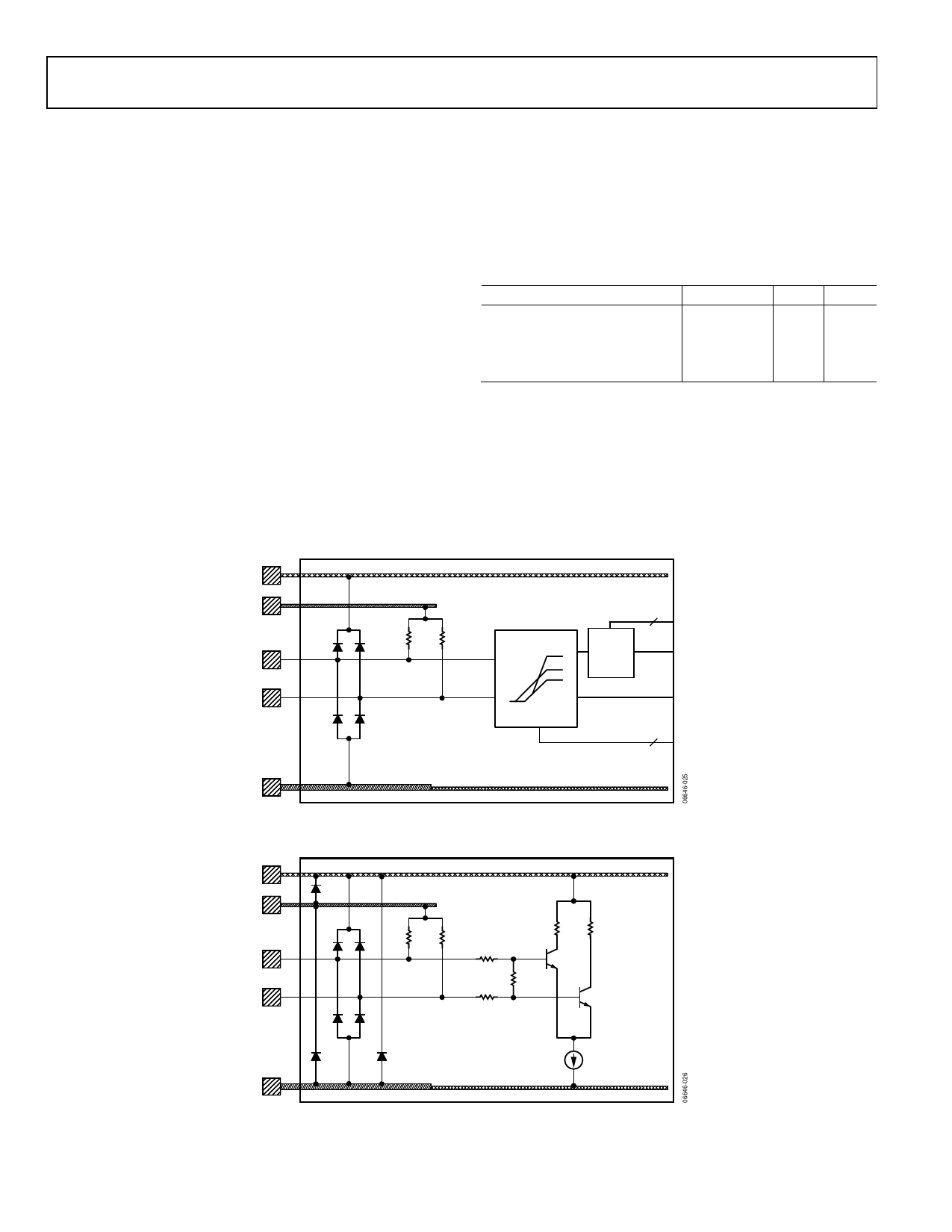
RECEIVERS
The AD8158 receivers incorporate 50 Ω on-chip termination,
ESD protection, and a multizero equalization function capable
of delivering up to 18 dB of boost at 4.25 GHz. The AD8158 can
compensate signal degradation at 6.5 Gbps from over 40 inches
of FR-4 backplane trace. The receive path also incorporates a
loss-of-signal (LOS) function with user programmable thresh-
old and hysteresis, which squelches the associated transmitter
when the midband differential voltage falls below a specified
threshold value. Finally, the receivers implement a sign-swapping
option (P/N swap), which allows the user to invert the sign of
the input signal path and eliminates the need for board-level
crossovers in the receive channels.
Input Structure and Allowed Input Levels
The AD8158 tolerates an input common-mode range (meas-
ured with zero differential input) of
VEE + 0.6 V < VIN_CM < VCC + 0.3 V
Typical supply configurations include, but are not limited to,
those listed in Table 11.
Table 11. Typical Input Supply Configurations
Configuration
DVCC
VCC
VTTI
Low VTTI, AC-Coupled Input
3.3 V − 1.8 V 1.8 V 1.6 V
Single 1.8 V Supply
3.3 V − 1.8 V 1.8 V 1.8 V
3.3 V Core
3.3 V
3.3 V 1.8 V
Single 3.3 V Supply
3.3 V
3.3 V 3.3 V
When dc-coupling with LVDS, CML, or ECL signals, it can be
advantageous to operate with split or negative supplies (see the
Applications Information section). In these applications, it is
necessary to observe the maximum voltage ratings between VCC
and VEE and generally to select supply voltages for VTTO and VTTI
in the range of VCC to VEE to avoid activating the ESD protection
devices.
VCC
VTTI
IP_xx
IN_xx
ESD
ON-CHIP TERMINATION
RP
RTERM
RN
RTERM
EQUALIZER
VTHRESH
LOSS
OF
SIG
SIGNAL
DETECT
EQ OUT
VEE
VCC
VTTI
IP_xx
IN_xx
VEE
Figure 37. Functional Diagram of the AD8158 Receiver
RLN
RLP
RP
RN
RL
RL
52Ω
52Ω R1
750Ω
Q1
R2
750Ω
R3
1kΩ
Q2
I1
Figure 38. Simplified Receiver Input Structure
Rev. 0 | Page 18 of 36
Share Link: 