P80C557E6 查看數據表(PDF) - Philips Electronics
零件编号
产品描述 (功能)
比赛名单
P80C557E6 Datasheet PDF : 64 Pages
| |||
Philips Semiconductors
Single-chip 8-bit microcontroller
Product specification
P83C557E6/P80C557E6
6.4 I/O Facilities
The P8xC557E6 has six 8–bit ports. Ports 0 to 3 are the same as in
the 80C51, with the exception of the additional functions of Port 1.
The parallel I/O function of Port 4 is equal to that of Ports 1, 2 and 3.
Port 5 has a parallel input port function, but has no function as an
output port.
The SDA and SCL lines serve the serial port SI01 (I2C). Because
the I2C–bus may be active while the device is disconnected from
VDD, these pins, are provided with open drain drivers.
Ports 0, 1, 2, 3, 4 and 5 perform the following alternative functions:
Port 0 :
Port 1 :
Port 2 :
Port 3 :
provides the multiplexed low–order address and
data bus used for expanding the P8xC557E6 with
standard memories and peripherals.
Port 1 is used for a number of special functions:
4 capture inputs (or external interrupt request inputs
if capture information is not utilized)
– external counter input
– external counter reset input
provides the high–order address bus when the
P8xC557E6 is expanded with external Program
Memory and/or external Data Memory.
pins can be configured individually to provide:
– external interrupt request inputs
– counter inputs
– receiver input and transmitter output of seri port
SIO 0 (UART)
– control signals to read and write external Data
Memory
Port 4 :
Port 5 :
can be configured to provide signals indicating a
match between timer counter T2 and its compare
registers.
may be used in conjunction with the ADC inter-
face.Unused analog inputs can be used as digital
inputs. As Port 5 lines may be used as inputs to the
ADC, these digital inputs have an inherent hystere-
sis to prevent the input logic from drawing too much
current from the power lines when driven by analog
signals. Channel to channel crosstalk should be tak-
en into consideration when both digital and analog
signals are simultaneously input to Port 5 (see DC
characteristics).
All ports are bidirectional with the exception of Port 5 which is an
input port.
Pins of which the alternative function is not used may be used as
normal bidirectional I/Os.
The generation or use of a Port 1, Port 3 or Port 4 pin as an
alternative function is carried out automatically by the P8xC557E6
provided the associated Special Function Register bit is set HIGH.
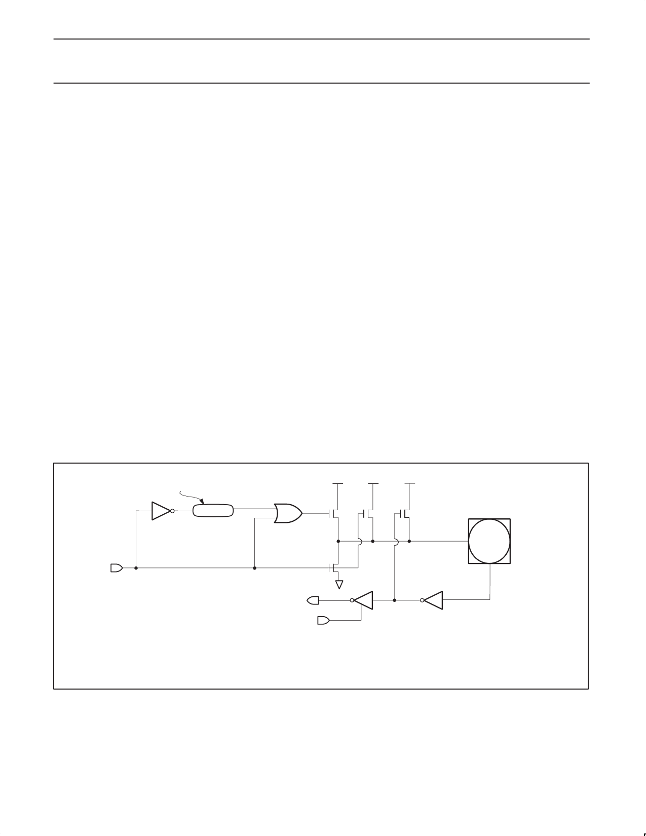
The pull–up arrangements of Ports 1 – 4 are shown in Figure 9.
2 System Clock Periods
VDD
VDD
VDD
P1
P2
P3
QN
From Port
Latch
Port
Pin
n
Input Data
Read Port Pin
P1 is turned on for 2 system clock periods after QN makes a 1–to–0 transition.
During this time, P1 also turns on P3 through the inverter to form an additional pull up.
Figure 9. I/O buffers in the P8xC557E6 (Ports 1, 2, 3 and 4).
1999 Mar 02
15
Share Link: 